Available For:

.jpg)








Key Features and Capabilities
Intuitive Hardware and Software Control
Reliable Low-Noise Electrical Measurements
Precision Fixture for Sample Loading
Precision Movable Electrical Probe for Site-Specific Characterization
Stable Electrical Contacts for High-Resolution Imaging
How it works
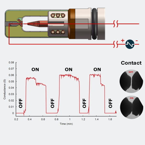
The TEM Biasing Nano-Manipulator Sample Holder combines a precision movable electrical probe, independent three-axis nanomanipulation, low-noise electrical connections, and an integrated source meter into a single platform for site-specific electrical characterization inside the TEM. Samples prepared on standard 3 mm half grids, FIB lift-out grids, or custom substrates are mounted in the removable sample cartridge using a dedicated setup block for accurate, repeatable assembly. The cartridge is then installed in the holder, automatically establishing electrical connections while leaving the measurement circuit open.
During the experiment, the movable probe is positioned using uncoupled piezo-driven coarse and fine motion along the X, Y, and Z axes until it contacts the specimen, completing the electrical circuit under direct TEM observation. Hummingbird Control™ Software provides an intuitive graphical user interface for precise probe control with configurable step sizes and integrated motion compensation to simplify contact formation and optimize probe positioning.
Once contact is established, researchers can apply electrical bias and acquire low-noise electrical measurements while simultaneously performing TEM/STEM imaging, electron diffraction, EDS, and EELS. The probe can be repositioned throughout the experiment to investigate multiple devices, interfaces, and regions within the same specimen, enabling flexible, site-specific electrical characterization in a single TEM session.