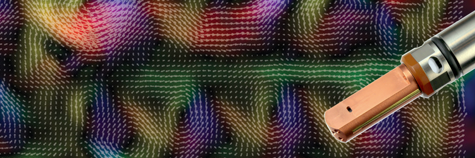

TEM Magnetizing
Available For:
.jpg)



Key Features and Capabilities
Calibrated In-Plane Applied Magnetic Field
Passive Beam Deflection Compensation
In-Stock Magnetizing Chips
Built for Diverse Applications
Featured Research
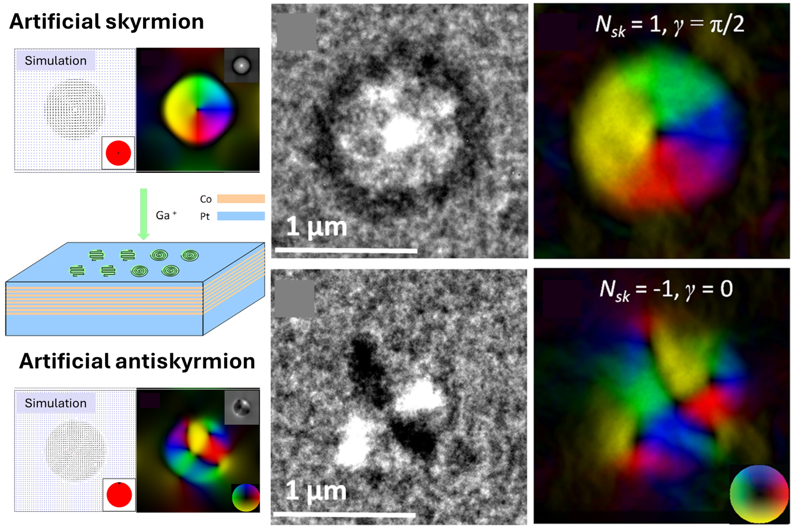
Artificial skyrmions and antiskyrmions in Co/Pt multilayers observed by in-situ magnetizing Lorentz TEM
Comparison of simulated (left) artificial skyrmions and antiskyrmions to real skyrmion (top)and antiskyrmion (bottom) domains imaged using Lorentz TEM. Inset schematic illustrates artificial engineering process using ion irradiation.
Reference: S. Zhang, et al. Scientific Reports (2016). DOI: 10.1038/srep31248
Copyright © 2016 The Author(s). Published by SpringerNature. This article is distributed under the terms of the Creative CommonsAttribution 4.0 International License (CC BY 4.0).
Selected Publications
Charudatta Phatak, John Fullerton, Hanu Arava. “Automated imaging of the annihilation of a transverse domain wall in patterned magnetic thin films”. APL Materials (2025)
V Brajuskovic, F Barrows, C Phatak, A K Petford-Long. “Real-space observation of magnetic excitations and avalanche behavior in artificial quasicrystal lattices”. Scientific Reports (2016)
S. Zhang, A. K. Petford-Long, C. Phatak. “Creation of artificial skyrmions and antiskyrmions by anisotropy engineering”. Scientific Reports (2016)
A. Budruk, C. Phatak, A.K. Petford-Long, M. De Graef. “In situ lorentz TEM magnetization study of a Ni-Mn-Ga ferromagnetic shape memory alloy”. Acta Materialia (2011)
A. Budruk, C. Phatak, A.K. Petford-Long, M. De Graef. “In situ Lorentz TEM magnetization studies on a Fe-Pd-Co martensitic alloy”. Acta Materialia (2011)