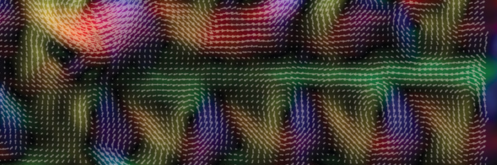
How do emergent quantum effects manifest nanoscale transformations?
Hummingbird Scientific in-situ holders enable real-time characterization of quantum materials under electrical bias or magnetic fields, connecting nanoscale transformations with material performance. Ultra-stable microfabricated chips support operando biasing TEM from −170 °C to above 1000 °C without drift correction. Scroll down to explore the quantum-material experiments enabled by these reproducible, easy-to-use systems.

Which type of experiment best matches your research?
Operando imaging of quantum effects at room temperature
Correlate charge transport mechanisms with nanoscale structural and electrical behavior in quantum materials.

Operando imaging of quantum effects at room temperature
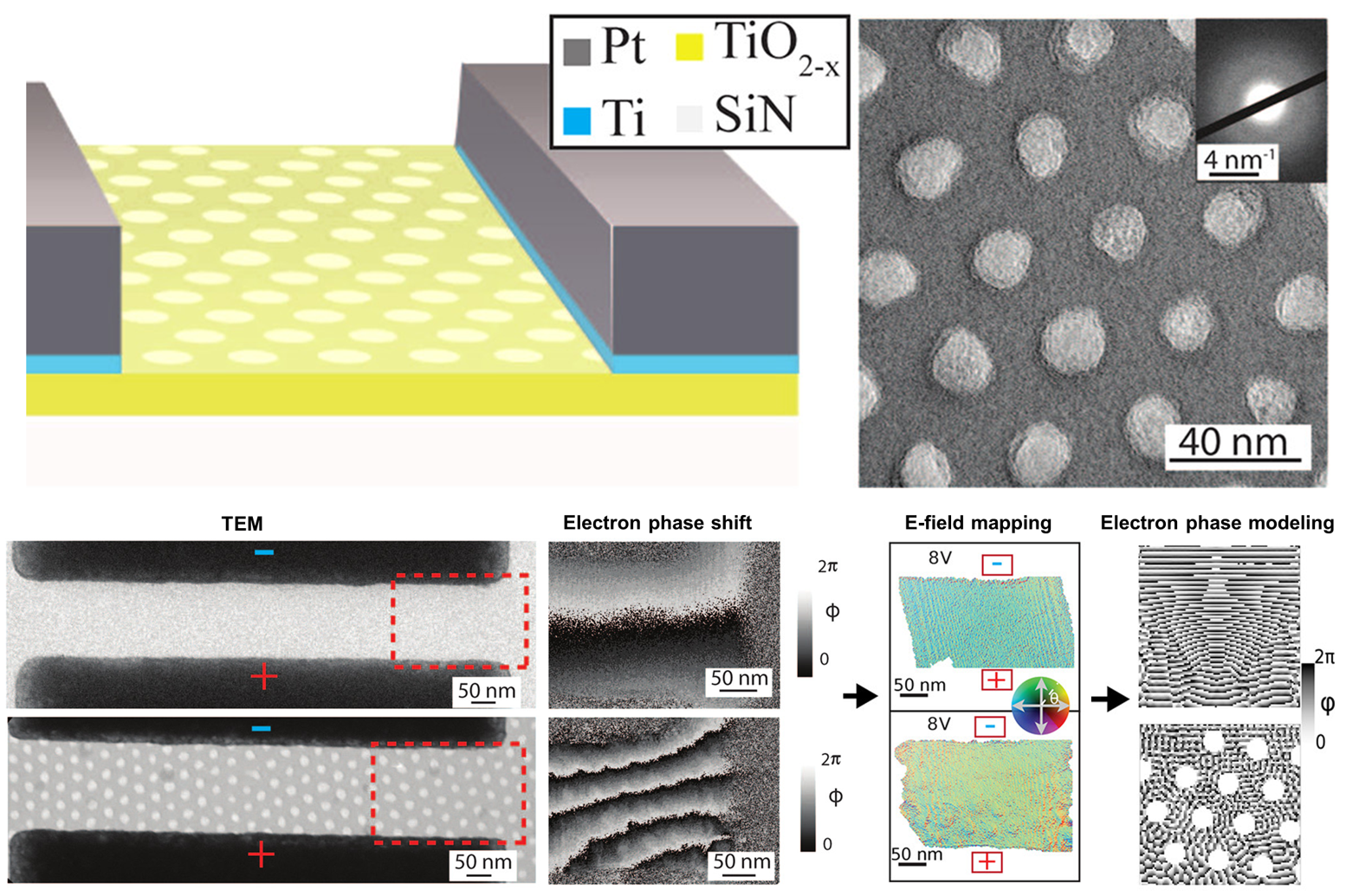
Confined electron and ion transport mechanisms in titania antidot thin films
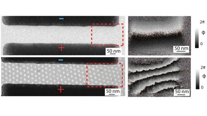
Titania thin films patterned with a lattice featuring 11-20 nm antidot features were characterized using in-situ electron holography and impedance spectroscopy to characterize charge transport dynamics.
- Voltage was applied in-situ to thin film sample using the biasing holder.
- Transport mechanism shifts from ion and vacancy motion to electron hopping due to room temperature quantum interference.
- Patterned films lacked hysteresis and filamentation effects characteristic of continuous films.
Reference: Frank Barrows, et al, ACS Nano 15, 8, 12935–12944 (2021) DOI: 10.1021/acsnano.1c01340
Image copyright © 2021 UChicago Argonne, LLC, Operator of Argonne National Laboratory. Published by American Chemical Society
Pre- and post-reaction TEM characterization
Correlate the three-dimensional structure and composition of quantum materials using electron tomography and atom probe tomography.
Pre- and post-reaction TEM characterization
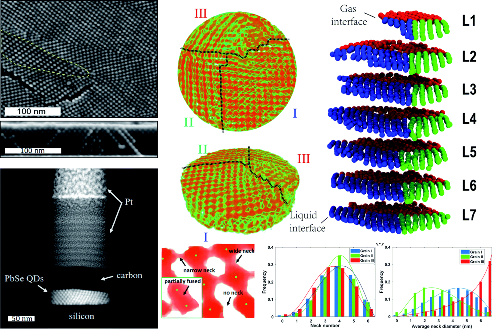
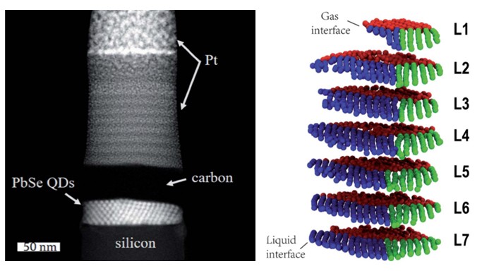
Transmission electron tomography of colloidal quantum dot superlattice
An epitaxially-fused polycrystalline PbSe quantum dot superlattice was characterized using HAADF-STEM electron tomography and reconstructed in 3D.
- All 1846 quantum dot centers-of-mass and necks were mapped in high resolution.
- The tomogram revealed three distinct superlattice grains with their effect on charge transport estimated using KMC
- High neck connectivity was correlated to local spatial order, defect incidence related to position within the superlattice.
Reference: Xiaolei Chu, et al, Journal of Materials Chemistry A. 8, 18254-18265 (2020) DOI: 10.1039/D0TA06704K
Image copyright © The Royal Society of Chemistry 2020
Operando imaging of quantum effects at room temperature
Correlate charge transport mechanisms with nanoscale structural and electrical behavior in quantum materials.
Pre- and post-reaction TEM characterization
Correlate the three-dimensional structure and composition of quantum materials using electron tomography and atom probe tomography.
Browse publications
Microscopy and Microanalysis
ACS Nano
ACS Nano
Journal of Materials Chemistry A
Research Spotlight
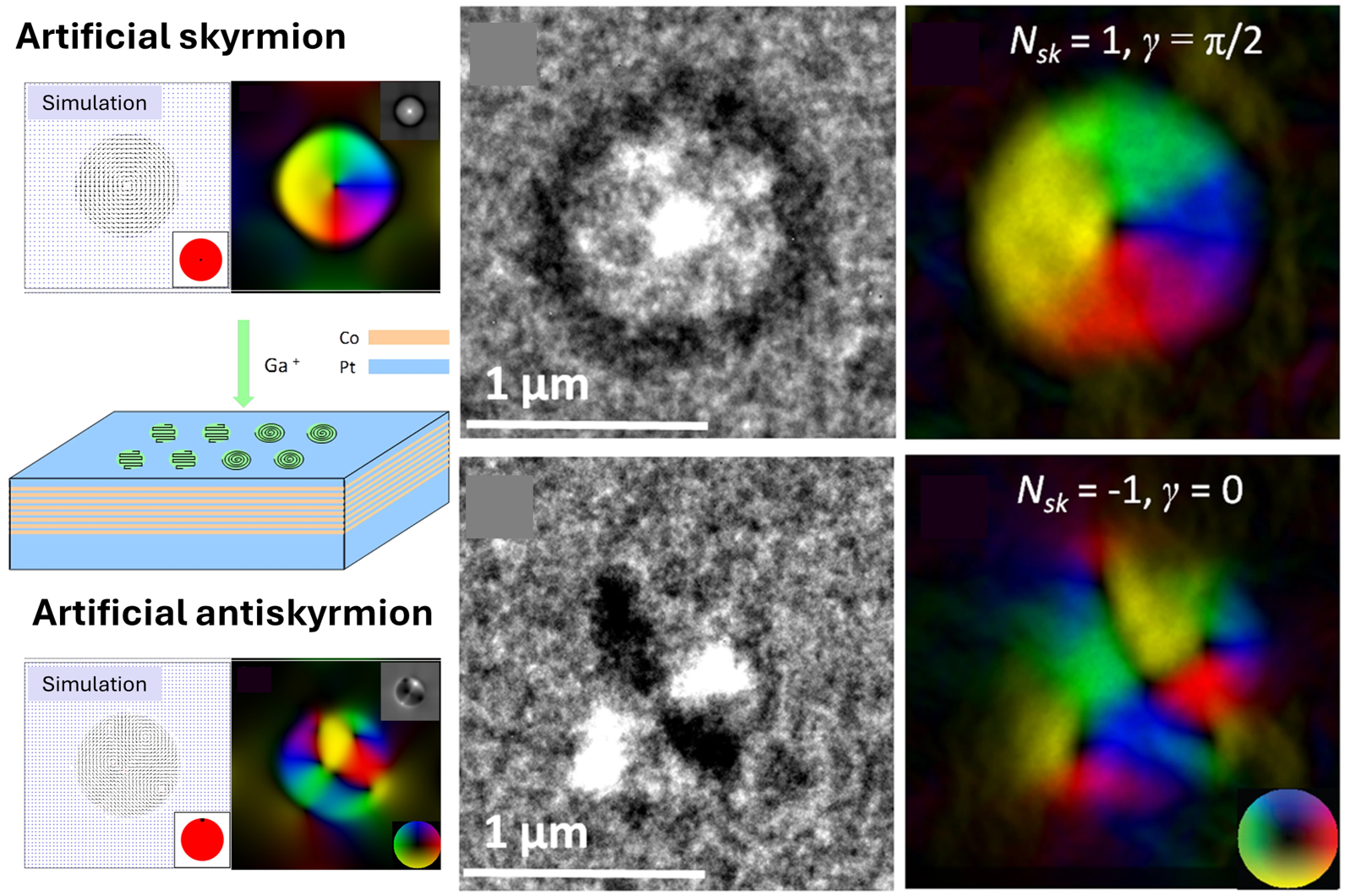
Comparison of simulated (left) artificial skyrmions and antiskyrmions to real skyrmion (top)and antiskyrmion (bottom) domains imaged using Lorentz TEM. Inset schematic illustrates artificial engineering process using ion irradiation.
Artificial skyrmions and antiskyrmions in Co/Pt multilayers observed by in-situ magnetizing Lorentz TEM
The Hummingbird Scientific TEM Magnetizing sample holder was used to investigate the magnetic stability and reversal behavior of artificially engineered skyrmions and antiskyrmions in ion-irradiated Co/Pt multilayer films. Combining in-situ magnetic field application with aberration-corrected Lorentz TEM, researchers directly observed the formation, evolution, and switching of topologically non-trivial spin textures under applied magnetic fields at room temperature. The holder enabled controlled manipulation of magnetic states while maintaining high-quality imaging, revealing how dipolar interactions stabilize artificial skyrmions and antiskyrmions without requiring Dzyaloshinskii–Moriya (DM) interactions. These observations provided key insight into the magnetic behavior of engineered spin textures relevant to future spintronic and magnonic devices.
Reference: S. Zhang, et al. Scientific Reports (2016). DOI: 10.1038/srep31248
Copyright © 2016 The Author(s). Published by SpringerNature. This article is distributed under the terms of the Creative CommonsAttribution 4.0 International License (CC BY 4.0).
Why choose Hummingbird Scientific for your research?
Hummingbird Scientific supports in situ and operando quantum materials research with flexible microscopy platforms, customizable sample chips, direct scientist support, internal TEM lab expertise, and in-house engineering and manufacturing capabilities.
Broader options for in situ quantum materials experiments
Quantum materials research often requires the application of electrical biasing, heating, cryogenic temperatures, magnetic fields, environmental control, or combined stimuli to investigate emergent electronic and magnetic phenomena. Hummingbird supports these studies with in situ TEM, SEM, and X-ray microscopy platforms for electrical biasing, cryo-biasing, heating, magnetizing, nano-manipulation, and air-free transfer, allowing researchers to match the experimental configuration to their material system and scientific objectives.
More chip choices for experimental flexibility
Microfabricated chip design plays a critical role in quantum materials experiments by defining the electrical configuration, thermal control, sample geometry, and analytical performance. With our dedicated in-house microfabrication division, Hummingbird develops standard and custom chips for electrical biasing, heating, window geometries, electrode layouts, and specialized sample architectures. This enables researchers to tailor the experimental platform to their quantum material system while maintaining compatibility across TEM, SEM, and synchrotron X-ray microscopy.
Scientist support backed by an internal TEM Lab
Quantum materials researchers work directly with scientists and technical staff who understand the practical details of in situ and operando TEM workflows. Hummingbird’s internal TEM Lab allows our team to evaluate microscope-facing performance during development, including alignment, handling, imaging stability, sample-environment behavior, and workflow usability under real TEM conditions.
Engineering, production, and custom capability
Hummingbird's in-house capabilities connect engineering, microfabrication, manufacturing, assembly, calibration, and testing within one development process. For quantum materials research, that means standard products can be supported by custom chips and holder configurations, and application-specific workflow changes when the experiment requires something more specific.
Operando imaging of quantum effects at room temperature
Correlate charge transport mechanisms with nanoscale structural and electrical behavior in quantum materials.
Operando imaging of quantum effects at room temperature
Confined electron and ion transport mechanisms in titania antidot thin films
Titania thin films patterned with a lattice featuring 11-20 nm antidot features were characterized using in-situ electron holography and impedance spectroscopy to characterize charge transport dynamics.
- Voltage was applied in-situ to thin film sample using the biasing holder.
- Transport mechanism shifts from ion and vacancy motion to electron hopping due to room temperature quantum interference.
- Patterned films lacked hysteresis and filamentation effects characteristic of continuous films.
Reference: Frank Barrows, et al, ACS Nano 15, 8, 12935–12944 (2021) DOI: 10.1021/acsnano.1c01340
Image copyright © 2021 UChicago Argonne, LLC, Operator of Argonne National Laboratory. Published by American Chemical Society
Pre- and post-reaction TEM characterization
Correlate the three-dimensional structure and composition of quantum materials using electron tomography and atom probe tomography.
Pre- and post-reaction TEM characterization
Transmission electron tomography of colloidal quantum dot superlattice
An epitaxially-fused polycrystalline PbSe quantum dot superlattice was characterized using HAADF-STEM electron tomography and reconstructed in 3D.
- All 1846 quantum dot centers-of-mass and necks were mapped in high resolution.
- The tomogram revealed three distinct superlattice grains with their effect on charge transport estimated using KMC
- High neck connectivity was correlated to local spatial order, defect incidence related to position within the superlattice.
Reference: Xiaolei Chu, et al, Journal of Materials Chemistry A. 8, 18254-18265 (2020) DOI: 10.1039/D0TA06704K
Image copyright © The Royal Society of Chemistry 2020
Featured products


Frequently asked questions
Ready to discuss your experiment?
Talk with an applications scientist to identify the right products for your experiment and request a quote.