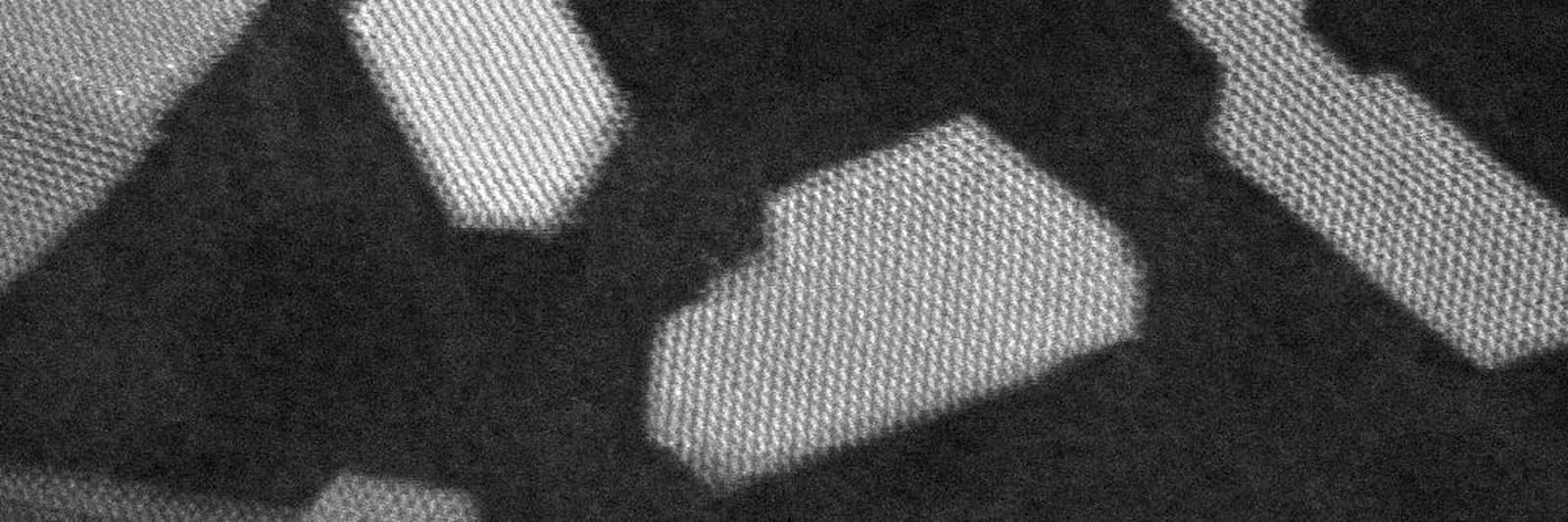
Curious how materials behave when dimensions shrink to the atomic limit?
Hummingbird Scientific in-situ sample holders support real-time, atomic-resolution characterization of low-dimensional materials, directly linking nanoscale structure to function. Conduct multimodal TEM, SEM, and X-ray experiments in gas, liquid, and vacuum environments, with closed-loop temperature control from −170 °C to above 1000 °C for studying material behavior under realistic conditions.
Precision-machined holders provide reproducibility, performance, and ease of use. Explore experiment examples below, with published research and compatible Hummingbird products.

Which type of experiment best matches your research?

2D materials dynamics in liquids
Capture molecular interactions and interfacial dynamics on 2D materials in liquid environments while directly observing nanoscale structural changes.

2D materials dynamics in liquids
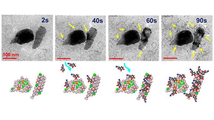
Direct visualization of biomolecule interactions at 2D materials surfaces
Interaction dynamics of norepinephrine molecules on 2D aluminum quasicrystals (Al-QCs) were imaged under liquid environment.
- Binding of norepinephrine to 2D Al-QCs imaged in real time.
- Initial binding occurred at the flake edge, then spread across the Al-QC surface.
- The findings pave the way for designing next-generation, highly selective electrochemical biosensors.
Reference: Anyesha Chakraborty, et al, ACS Appl. Mater. Interfaces 17, 68552−68565 (2025). DOI: 10.1021/acsami.5c10972
Image copyright © 2025 American Chemical Society

2D material at high temperatures
Observe phase transformations, structural evolution, and thermal stability of 2D materials at elevated temperatures.
2D material at high temperatures
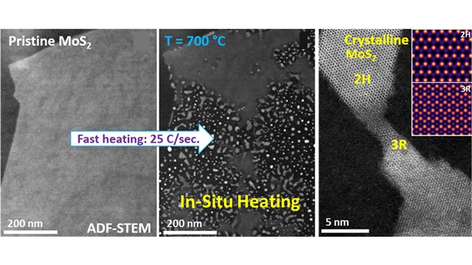
In-situ observations of non-equilibrium phase changes in 2D materials
Phase transformation in 2D MoS2 under non-equilibrium thermodynamics conditions were observed using in-situ aberration-corrected STEM.
- Fast in-situ heating at 25 °C/sec to 700 °C yielded highly ordered hexagonal MoS2 crystal islands less than 20 nm in size.
- Slow ex-situ heating at 25 °C/min yielded nanocrystalline and sub-stoichiometric amorphous regions.
- The results present a new way to synthesize atomically thin, confined nanostructures for electronics applications.
Reference: Pawan Kumar, et al, npj 2D Mater Appl 4, 16 (2020). DOI: 10.1038/s41699-020-0150-2
Image from npj 2D Materials and Applications under the Creative Commons license

2D materials-based electronic devices
Correlate electrical transport with nanoscale structural evolution in operating 2D materials-based devices.
2D materials-based electronic devices
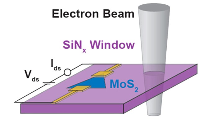
In-Situ TEM of an electron beam gated 2D MoS2 field-effect transistor
Electrical gating of 2D MoS2 channels was achieved using the TEM electron beam during operando biasing measurements.
- Electron-beam irradiation of the supporting SiNx membrane induced surface charging, reducing MoS₂ conductance by up to 94%.
- The effect was reversible, with on/off ratios reaching 56 at higher beam currents.
- The results demonstrate beam-induced substrate charging as a controllable gate for in situ study of 2D nanoelectronic devices without complex fabrication.
Reference: Paul Masih Das & Marija Drndić, ACS Nano 14, 6, 7389-7397 (2020). DOI: 10.1021/acsnano.0c02908
Image copyright © 2020 American Chemical Society

Low dimensional materials growth in gas environment
Capture low dimensional material nucleation, growth, and morphology evolution during gas-phase synthesis.
Low dimensional materials growth in gas environment
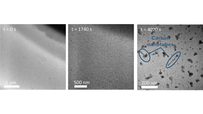
In-situ chemical vapor deposition (CVD) of carbon nanotubes (CNT) and nanofibers (CNF)
The effect of different Fe-based alloy catalyst systems on in-situ atmospheric pressure CVD of CNTs and CNFs was characterized.
- Fe, Fe + Na2CO3, and stainless-steel catalysts were evaluated at 775º C under H2/C2H4 (5:2) flow (up to 5 sccm) for in-situ CNT/CNF growth.
- Na2CO3 (desiccant effect) and Cr in stainless steel (oxygen scavenging) significantly enhanced CNT/CNF yield.
- EDS and EELS confirmed oxygen capture by chromium in stainless steel.
- The results provide pathways to optimize growth and enable deeper insight into CVD processes.
Reference: Andrew C. Meng, et al, J. Vac. Sci. Technol. B 43, 040601 (2025). DOI: 10.1116/6.0004664
Image copyright © 2026 AIP Publishing LLC

Low dimensional materials growth in liquids
Study the growth dynamics and structural evolution of low-dimensional materials under liquid-phase conditions.
Low dimensional materials growth in liquids
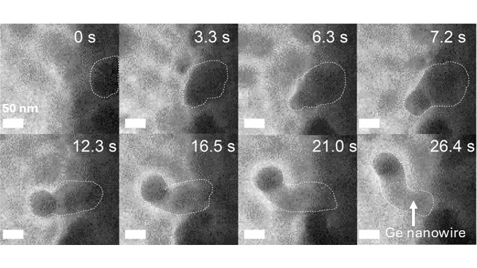
In-situ liquid phase growth of Ge nanowires from liquid metal nanodroplets
Room-temperature Ge nanowire growth in water was directly visualized using in-situ liquid phase TEM, where electron beam interaction with liquid Ga or In nanodroplets initiated localized nucleation and growth.
- Electron beam–induced electrochemical liquid–liquid–solid (ec-LLS) growth from liquid metal nanodroplets was observed without external biasing.
- Growth occurred only within a narrow parameter window: intermediate ligand coverage, GeO2 >5 mM, sufficient droplet density, and a beam current density threshold (~8 nA μm⁻²).
- The findings establish a pathway for radiolysis-driven “wireless” growth and broader in-situ studies of nanomaterial formation and liquid metal–electrolyte interfaces.
Reference: Quintin Cheek, et al, ACS Nano 14, 3, 2869-2879 (2020). DOI: 10.1021/acsnano.9b06468
Image copyright © 2020 American Chemical Society

Low dimensional materials decomposition in gas
Observe thermal decomposition, phase evolution, and structural transformations of low-dimensional materials under reactive gas environments.
Low dimensional materials decomposition in gas
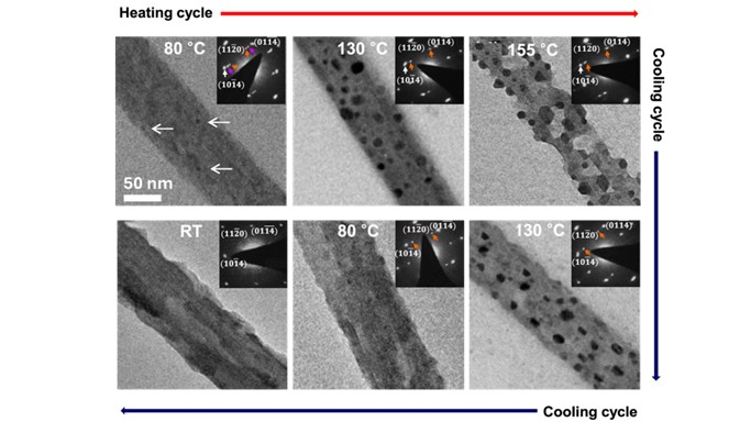
Reversible in-situ gas phase thermal decomposition of perovskite nanorods
Evolution of single-crystal nanorods of intermediate phase (MAI-PbI2-DMSO) was observed under controlled thermal conditions.
- Gas-phase annealing at ~10⁻² Torr with thermal cycling up to ~165 °C enabled tracking of phase evolution during decomposition.
- Decomposition into PbI2 increased rapidly with temperature and continued cooling, indicating irreversible, gas interaction-driven degradation pathways.
- These findings link phase evolution and thermal decomposition to charge transport, enabling optimized processing and scalable, high-performance flexible devices.
Reference: Yong-Ryun Jo, et al, ACS Cent. Sci. 6, 6, 959-968 (2020). DOI: 10.1021/acscentsci.0c00385
Image copyright © 2020 American Chemical Society

Low dimensional materials decomposition in liquids
Investigate liquid-phase dissolution, defect evolution, and structural stability of low-dimensional materials.
Low dimensional materials decomposition in liquids
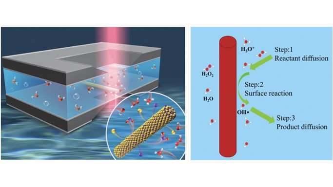
In-situ imaging of InAs nanowire dissolution in radiolytic water
The dissolution dynamics of InAs nanowires were directly visualized in a liquid environment to elucidate the underlying nanoscale dissolution mechanisms.
- MBE-grown (defect-free) and MOCVD-grown (stacking fault-rich) nanowires with diameters up to 50 nm were investigated.
- MBE nanowires start to dissolve immediately at a slower rate upon e-beam exposure, while MOCVD nanowires show delayed onset (~110 s) but dissolve more rapidly.
- The results indicate a surface reaction-limited dissolution mechanism, linking crystal defects to nanowire stability.
Reference: Mei Sun, et al, Nanoscale 10, 19733-19741 (2018). DOI: 10.1039/C8NR04096F
Image copyright © 2018 Royal Society of Chemistry
Manipulation and Biasing of Low Dimensional Materials
Probe targeted regions of low-dimensional materials to correlate electrical behavior with nanoscale structural evolution.
Manipulation and Biasing of Low Dimensional Materials
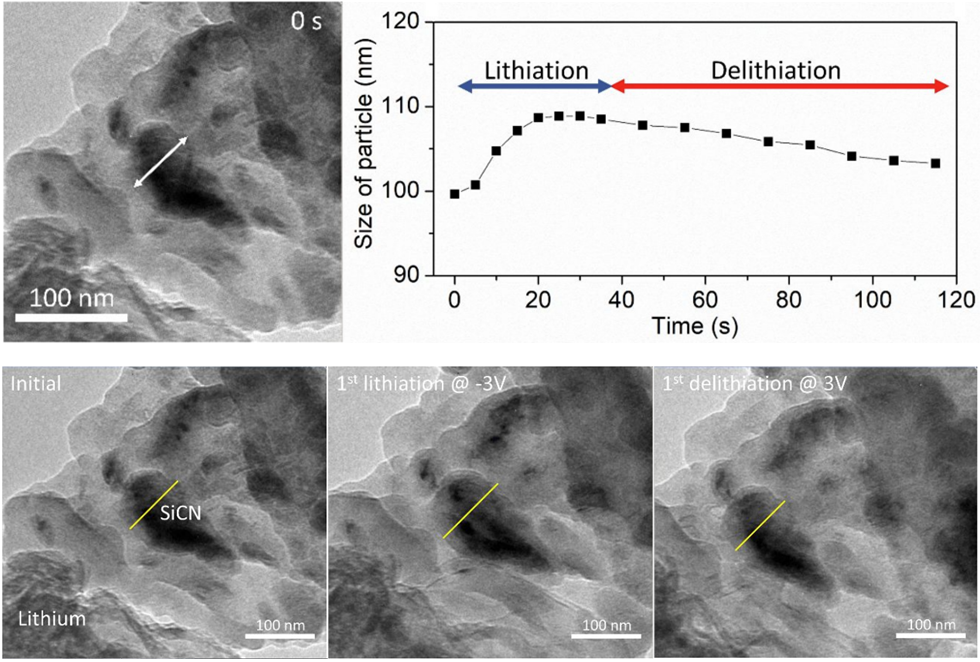
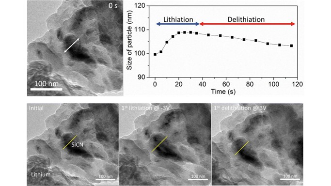
In-situ probing and site-specific biasing of graphene oxide-based nanocomposites
Microstructural evolution of a polymer-derived ceramic nanoparticle/edge-functionalized graphene oxide composite during lithiation–delithiation was directly imaged.
- Lithiation and delithiation were driven via constant biasing at −3.0 V and +3.0 V, respectively.
- The composite exhibited high structural stability, with only 9.36% linear expansion during lithiation.
- The study demonstrates site-specific in-situ probing and localized biasing to inform the design of next-generation battery materials.
Reference: Zeyang Zhang, et al, ACS Appl. Mater. Interfaces 13, 8, 9794-9803 (2021). DOI: 10.1021/acsami.0c19681
Image copyright © 2021 American Chemical Society

Low dimensional materials electrochemistry
Investigate electrochemical reactions, charge transfer, and structural evolution in low-dimensional materials under liquid environments.
Low dimensional materials electrochemistry
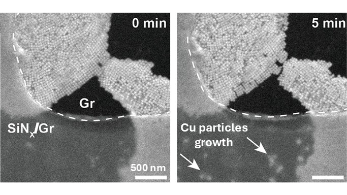
Evaluation of graphene electrodes for in-situ liquid phase electrochemistry
The performance of a graphene working electrode for CO2 electroreduction (CO2ER) of Cu nanocatalysts was evaluated via liquid phase SEM (LP-SEM).
- CV/CA and operando LP-SEM were conducted in CO₂-saturated 0.1 M KHCO3 from OCV to −1.1 V vs RHE, with potential holds between −0.8 and −1.1 V.
- Graphene exhibited a wider inert window of −0.69 V vs −0.52 V for glassy carbon and efficient charge transfer, enabling direct, real-time tracking of Cu redox, dissolution, and redeposition.
- The findings establish graphene as a stable, low-background platform for operando LP-S/TEM, linking electrochemical activity to nanoscale dynamics.
Reference: Saltanat Toleukhanova, et al, Adv. Mater. 36, 2311133 (2024). DOI: 10.1002/adma.202311133
Image from Advanced Materials under the Creative Commons license
2D materials dynamics in liquids
Capture molecular interactions and interfacial dynamics on 2D materials in liquid environments while directly observing nanoscale structural changes.
2D material at high temperatures
Observe phase transformations, structural evolution, and thermal stability of 2D materials at elevated temperatures.
2D materials-based electronic devices
Correlate electrical transport with nanoscale structural evolution in operating 2D materials-based devices.
Low dimensional materials growth in gas environment
Capture low dimensional material nucleation, growth, and morphology evolution during gas-phase synthesis.
Low dimensional materials growth in liquids
Study the growth dynamics and structural evolution of low-dimensional materials under liquid-phase conditions.
Low dimensional materials decomposition in gas
Observe thermal decomposition, phase evolution, and structural transformations of low-dimensional materials under reactive gas environments.
Low dimensional materials decomposition in liquids
Investigate liquid-phase dissolution, defect evolution, and structural stability of low-dimensional materials.
Manipulation and Biasing of Low Dimensional Materials
Probe targeted regions of low-dimensional materials to correlate electrical behavior with nanoscale structural evolution.
Low dimensional materials electrochemistry
Investigate electrochemical reactions, charge transfer, and structural evolution in low-dimensional materials under liquid environments.
Browse publications
Applied Catalysis B: Environment and Energy
Journal of Hazardous Materials
ACS Applied Materials & Interfaces
Journal of Vacuum Science \& Technology B
Research Spotlight
Rapid phase transformation of 2D PtSe2 into a Se-deficient PtSe1-x phase along a propagation front during in-situ heating, captured with a high-frame rate camera.
2D materials phase transformation at high temperatures
Two-dimensional (2D) PtSe₂ offers tunable band gaps for near-infrared optoelectronics, with properties highly sensitive to layer thickness, phase, and defects—making precise characterization essential, as subtle structural variations directly impact electronic and optical performance. The Hummingbird Scientific MEMS heating + biasing sample holder enables real-time, in situ control of these properties by applying high temperatures and electrical bias inside the TEM, driving phase transformations while maintaining atomic-resolution imaging.
The video captures the real-time transformation of 2D PtSe₂ into Se-deficient PtSe₁-x during in situ heating to ~550 °C, with the phase transition initiating near 500 °C. Evolving contrast reveals directional phase propagation and dynamic interfaces, providing direct insight into transformation pathways. The growth kinetics—and resulting phase front velocity—are tunable via the applied stimulus, enabling precise nanoscale control over phase engineering.
Hummingbird Advantages
- MEMS-based closed-loop sample heating beyond 1000 ºC.
- Near drift-free in-situ atomic-resolution imaging throughout the temperature range.
Reference: Data provided by Pawan Kumar, Eric Stach and Deep Jariwala from the University of Pennsylvania
Why choose Hummingbird Scientific for your research?
Hummingbird Scientific supports in situ low-dimensional materials research with flexible microscopy platforms, customizable sample chips, direct scientist support, internal TEM lab expertise, and in-house engineering and manufacturing capabilities.
Broader options for in situ low-dimensional materials experiments
Low-dimensional materials research spans a wide range of material systems, including graphene, transition metal dichalcogenides (TMDs), hexagonal boron nitride (hBN), MXenes, carbon nanotubes, nanowires, quantum dots, and van der Waals heterostructures. Understanding and engineering their properties for next-generation functional materials often requires characterization under electrical, thermal, cryogenic, gaseous, liquid, or other controlled conditions. Hummingbird supports these studies with in situ TEM, SEM, and X-ray microscopy platforms for electrical biasing, heating, cryo-biasing, gas and liquid environments, nano-manipulation, and air-free transfer, enabling researchers to match the experimental platform to their material system and research objectives.
More chip choices for experimental flexibility
Microfabricated chip design is fundamental to experiments on low-dimensional materials. Through our dedicated microfabrication division, Hummingbird develops standard and custom chips for electrical biasing, heating, liquid-flow and gas-cell experiments, with configurable electrode layouts, spacer thicknesses, window geometries, and specialized sample architectures. This flexibility allows researchers to tailor the experimental platform to their material system while maintaining compatibility across TEM, SEM, and synchrotron X-ray microscopy
Scientist support backed by an internal TEM Lab
Low-dimensional materials researchers work directly with scientists and technical staff who understand the practical details of in situ and operando TEM workflows. Hummingbird’s internal TEM Lab allows our team to evaluate microscope-facing performance during development, including alignment, handling, imaging stability, sample-environment behavior, and workflow usability under real TEM conditions.
Engineering, production, and custom capability
Hummingbird's in-house capabilities connect engineering, microfabrication, manufacturing, assembly, calibration, and testing within one development process. For low-dimensional materials research, that means standard products can be supported by custom chips and holder configurations, and application-specific workflow changes when the experiment requires something more specific.
2D materials dynamics in liquids
Capture molecular interactions and interfacial dynamics on 2D materials in liquid environments while directly observing nanoscale structural changes.
2D materials dynamics in liquids
Direct visualization of biomolecule interactions at 2D materials surfaces
Interaction dynamics of norepinephrine molecules on 2D aluminum quasicrystals (Al-QCs) were imaged under liquid environment.
- Binding of norepinephrine to 2D Al-QCs imaged in real time.
- Initial binding occurred at the flake edge, then spread across the Al-QC surface.
- The findings pave the way for designing next-generation, highly selective electrochemical biosensors.
Reference: Anyesha Chakraborty, et al, ACS Appl. Mater. Interfaces 17, 68552−68565 (2025). DOI: 10.1021/acsami.5c10972
Image copyright © 2025 American Chemical Society
2D material at high temperatures
Observe phase transformations, structural evolution, and thermal stability of 2D materials at elevated temperatures.
2D material at high temperatures
In-situ observations of non-equilibrium phase changes in 2D materials
Phase transformation in 2D MoS2 under non-equilibrium thermodynamics conditions were observed using in-situ aberration-corrected STEM.
- Fast in-situ heating at 25 °C/sec to 700 °C yielded highly ordered hexagonal MoS2 crystal islands less than 20 nm in size.
- Slow ex-situ heating at 25 °C/min yielded nanocrystalline and sub-stoichiometric amorphous regions.
- The results present a new way to synthesize atomically thin, confined nanostructures for electronics applications.
Reference: Pawan Kumar, et al, npj 2D Mater Appl 4, 16 (2020). DOI: 10.1038/s41699-020-0150-2
Image from npj 2D Materials and Applications under the Creative Commons license
2D materials-based electronic devices
Correlate electrical transport with nanoscale structural evolution in operating 2D materials-based devices.
2D materials-based electronic devices
In-Situ TEM of an electron beam gated 2D MoS2 field-effect transistor
Electrical gating of 2D MoS2 channels was achieved using the TEM electron beam during operando biasing measurements.
- Electron-beam irradiation of the supporting SiNx membrane induced surface charging, reducing MoS₂ conductance by up to 94%.
- The effect was reversible, with on/off ratios reaching 56 at higher beam currents.
- The results demonstrate beam-induced substrate charging as a controllable gate for in situ study of 2D nanoelectronic devices without complex fabrication.
Reference: Paul Masih Das & Marija Drndić, ACS Nano 14, 6, 7389-7397 (2020). DOI: 10.1021/acsnano.0c02908
Image copyright © 2020 American Chemical Society
Low dimensional materials growth in gas environment
Capture low dimensional material nucleation, growth, and morphology evolution during gas-phase synthesis.
Low dimensional materials growth in gas environment
In-situ chemical vapor deposition (CVD) of carbon nanotubes (CNT) and nanofibers (CNF)
The effect of different Fe-based alloy catalyst systems on in-situ atmospheric pressure CVD of CNTs and CNFs was characterized.
- Fe, Fe + Na2CO3, and stainless-steel catalysts were evaluated at 775º C under H2/C2H4 (5:2) flow (up to 5 sccm) for in-situ CNT/CNF growth.
- Na2CO3 (desiccant effect) and Cr in stainless steel (oxygen scavenging) significantly enhanced CNT/CNF yield.
- EDS and EELS confirmed oxygen capture by chromium in stainless steel.
- The results provide pathways to optimize growth and enable deeper insight into CVD processes.
Reference: Andrew C. Meng, et al, J. Vac. Sci. Technol. B 43, 040601 (2025). DOI: 10.1116/6.0004664
Image copyright © 2026 AIP Publishing LLC
Low dimensional materials growth in liquids
Study the growth dynamics and structural evolution of low-dimensional materials under liquid-phase conditions.
Low dimensional materials growth in liquids
In-situ liquid phase growth of Ge nanowires from liquid metal nanodroplets
Room-temperature Ge nanowire growth in water was directly visualized using in-situ liquid phase TEM, where electron beam interaction with liquid Ga or In nanodroplets initiated localized nucleation and growth.
- Electron beam–induced electrochemical liquid–liquid–solid (ec-LLS) growth from liquid metal nanodroplets was observed without external biasing.
- Growth occurred only within a narrow parameter window: intermediate ligand coverage, GeO2 >5 mM, sufficient droplet density, and a beam current density threshold (~8 nA μm⁻²).
- The findings establish a pathway for radiolysis-driven “wireless” growth and broader in-situ studies of nanomaterial formation and liquid metal–electrolyte interfaces.
Reference: Quintin Cheek, et al, ACS Nano 14, 3, 2869-2879 (2020). DOI: 10.1021/acsnano.9b06468
Image copyright © 2020 American Chemical Society
Low dimensional materials decomposition in gas
Observe thermal decomposition, phase evolution, and structural transformations of low-dimensional materials under reactive gas environments.
Low dimensional materials decomposition in gas
Reversible in-situ gas phase thermal decomposition of perovskite nanorods
Evolution of single-crystal nanorods of intermediate phase (MAI-PbI2-DMSO) was observed under controlled thermal conditions.
- Gas-phase annealing at ~10⁻² Torr with thermal cycling up to ~165 °C enabled tracking of phase evolution during decomposition.
- Decomposition into PbI2 increased rapidly with temperature and continued cooling, indicating irreversible, gas interaction-driven degradation pathways.
- These findings link phase evolution and thermal decomposition to charge transport, enabling optimized processing and scalable, high-performance flexible devices.
Reference: Yong-Ryun Jo, et al, ACS Cent. Sci. 6, 6, 959-968 (2020). DOI: 10.1021/acscentsci.0c00385
Image copyright © 2020 American Chemical Society
Low dimensional materials decomposition in liquids
Investigate liquid-phase dissolution, defect evolution, and structural stability of low-dimensional materials.
Low dimensional materials decomposition in liquids
In-situ imaging of InAs nanowire dissolution in radiolytic water
The dissolution dynamics of InAs nanowires were directly visualized in a liquid environment to elucidate the underlying nanoscale dissolution mechanisms.
- MBE-grown (defect-free) and MOCVD-grown (stacking fault-rich) nanowires with diameters up to 50 nm were investigated.
- MBE nanowires start to dissolve immediately at a slower rate upon e-beam exposure, while MOCVD nanowires show delayed onset (~110 s) but dissolve more rapidly.
- The results indicate a surface reaction-limited dissolution mechanism, linking crystal defects to nanowire stability.
Reference: Mei Sun, et al, Nanoscale 10, 19733-19741 (2018). DOI: 10.1039/C8NR04096F
Image copyright © 2018 Royal Society of Chemistry
Manipulation and Biasing of Low Dimensional Materials
Probe targeted regions of low-dimensional materials to correlate electrical behavior with nanoscale structural evolution.
Manipulation and Biasing of Low Dimensional Materials
In-situ probing and site-specific biasing of graphene oxide-based nanocomposites
Microstructural evolution of a polymer-derived ceramic nanoparticle/edge-functionalized graphene oxide composite during lithiation–delithiation was directly imaged.
- Lithiation and delithiation were driven via constant biasing at −3.0 V and +3.0 V, respectively.
- The composite exhibited high structural stability, with only 9.36% linear expansion during lithiation.
- The study demonstrates site-specific in-situ probing and localized biasing to inform the design of next-generation battery materials.
Reference: Zeyang Zhang, et al, ACS Appl. Mater. Interfaces 13, 8, 9794-9803 (2021). DOI: 10.1021/acsami.0c19681
Image copyright © 2021 American Chemical Society
Low dimensional materials electrochemistry
Investigate electrochemical reactions, charge transfer, and structural evolution in low-dimensional materials under liquid environments.
Low dimensional materials electrochemistry
Evaluation of graphene electrodes for in-situ liquid phase electrochemistry
The performance of a graphene working electrode for CO2 electroreduction (CO2ER) of Cu nanocatalysts was evaluated via liquid phase SEM (LP-SEM).
- CV/CA and operando LP-SEM were conducted in CO₂-saturated 0.1 M KHCO3 from OCV to −1.1 V vs RHE, with potential holds between −0.8 and −1.1 V.
- Graphene exhibited a wider inert window of −0.69 V vs −0.52 V for glassy carbon and efficient charge transfer, enabling direct, real-time tracking of Cu redox, dissolution, and redeposition.
- The findings establish graphene as a stable, low-background platform for operando LP-S/TEM, linking electrochemical activity to nanoscale dynamics.
Reference: Saltanat Toleukhanova, et al, Adv. Mater. 36, 2311133 (2024). DOI: 10.1002/adma.202311133
Image from Advanced Materials under the Creative Commons license
Featured products




Frequently asked questions
Ready to discuss your experiment?
Talk with an applications scientist to identify the right products for your experiment and request a quote.