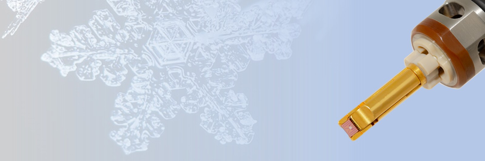

TEM Cryo Biasing + Heating
Perform variable-temperature in-situ TEM with closed-loop temperature control from <−170 °C to >1000 °C, screw-free direct MEMS chip loading, and 9 electrical contacts for on-chip heating and electrical biasing.
Technical Specs
1950 Series
Sample Temperature Range
~-170 °C to > 1000 °C
Temperature Control
Yes
Dewar Lifetime to Refill
4 hours
Number of Electrical Contacts
9
Contact Type
Direct Chip Contact
Settled Resolution at Minimum Temperature
Up to TEM resolution
EELS / EDS Compatible
Yes
Available For:


.jpg)
www.hummingbirdscientific.com ©Hummingbird Scientific 2026 -The specifications provided are subject to change without notice.

Key Features and Capabilities
Cryogenic Cooling for Stable In-Situ Characterization
Perform stable electrical biasing experiments at cryogenic temperatures with precise temperature control
Screw-Free Direct Chip Insertion
Load MEMS chips quickly with reliable electrical contact and simplified experiment setup
Nine Low-Noise Electrical Contacts
Perform low-noise in-situ electrical measurements with nine direct chip electrical contacts and individually shielded coaxial cables
60+ In-Stock TEM Heating and Biasing Chip Configurations
Keep experiments moving with in-stock MEMS chips for heating, electrical biasing, and advanced in-situ TEM characterization
Stable Imaging and Analytical Compatibility at Low Temperature
Maintain stable imaging with EDS and EELS compatibility throughout cryogenic in-situ TEM experiments
Integrated Heating
Optional add on
Expand from cryogenic cooling to variable-temperature electrical biasing with integrated MEMS heating to > 1000 °C
www.hummingbirdscientific.com ©Hummingbird Scientific 2026 -The specifications provided are subject to change without notice.
Built for Diverse Applications
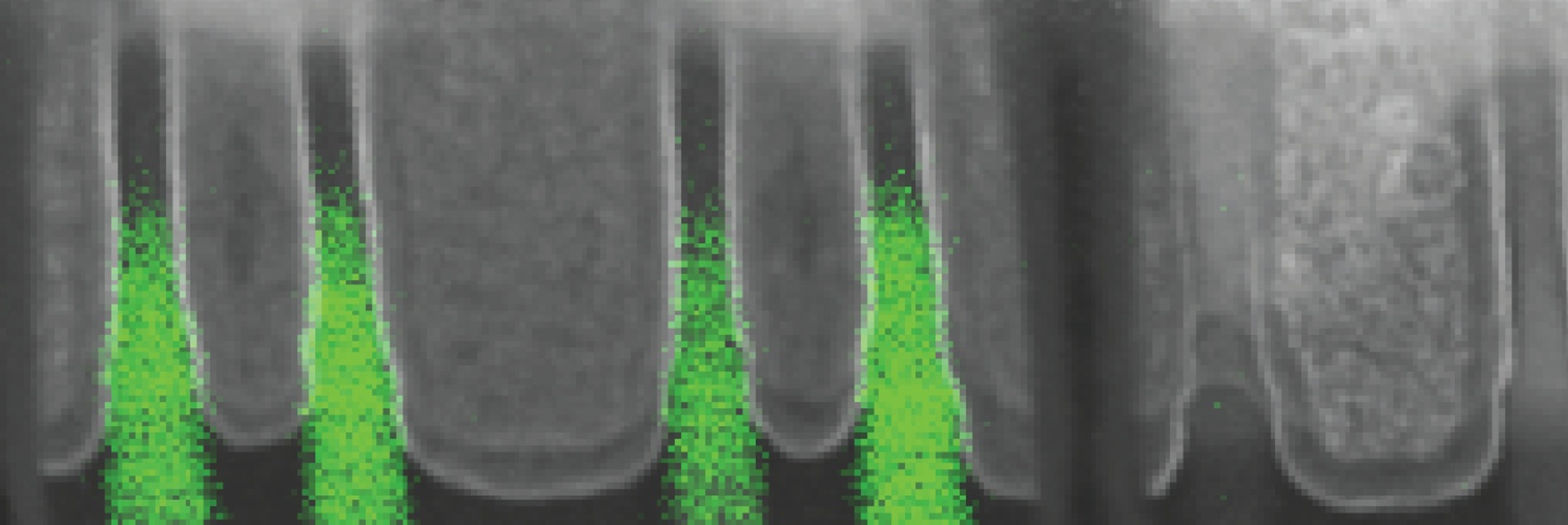


Featured Research
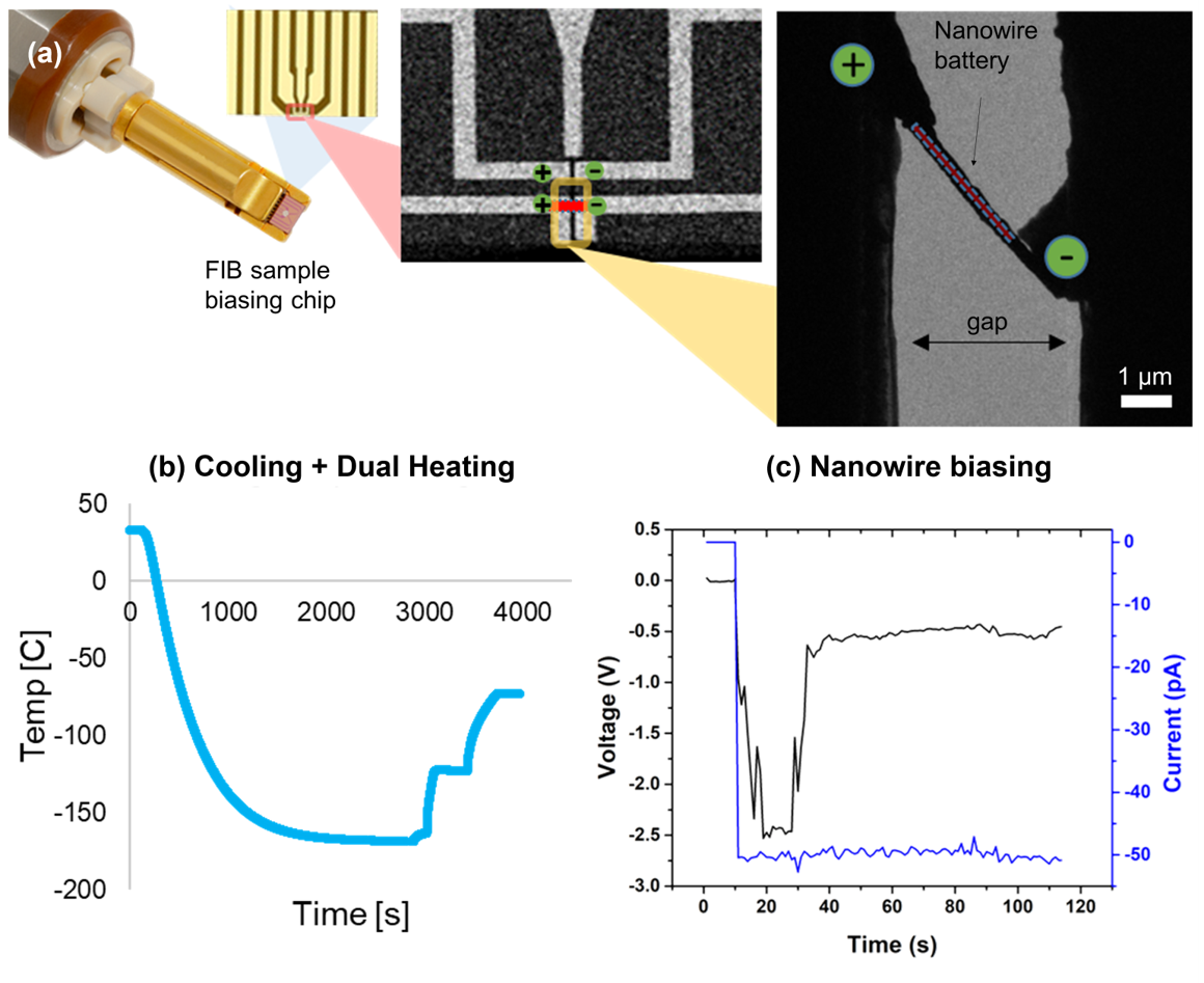
In-situ biasing of a nanowire at cryogenic temperature during dendrite plating reaction
a) Multi-scale schematic showing cryo biasing holder tip, FIB chip, and mounted nanowire sample. b) LN2 cooling and dual heating function to access intermediate temperatures between-170 °C and room temperature. c) Current response at cryogenic temperature following the plating of a dendrite layer on the surface of the nanowire.
Reference: Internal Collaboration withUCSD/Battery500 Consortium
www.hummingbirdscientific.com ©Hummingbird Scientific 2026 -The specifications provided are subject to change without notice.
www.hummingbirdscientific.com ©Hummingbird Scientific 2026 -The specifications provided are subject to change without notice.
Selected Publications
Khim Karki, Daan Hein Alsem, Norman Salmon. “Cryo-Electrical Microscopy for Quantum and Advanced Energy Applications”. Microscopy and Microanalysis (2021)
DOI:
10.1017/S143192762100859X


Visit our Website