In-House Microfabrication for In Situ TEM, SEM, X-ray, Cryo-EM, and OEM Development
Hummingbird Scientific designs, produces, inspects, and supports microfabricated chips and devices for advanced in situ microscopy workflows.
Our in-house microfabrication capability supports liquid cell TEM, gas cell TEM, heating, biasing, electrochemistry, magnetizing, X-ray microscopy, SEM liquid flow, cryo-EM workflow development, Fast Freezing prototype development, and custom OEM platforms.
With 150,000+ microfabricated chips produced, 60+ standard chip varieties, 20+ years of in situ microscopy development experience, and hundreds of custom chip designs, Hummingbird gives researchers and partners a proven foundation for chip-based microscopy experiments.

Microfabricated chips and devices
Hummingbird produces standard and custom microfabricated chips for liquid cell, heating, biasing, electrochemistry, gas, magnetizing, X-ray, and cryogenic microscopy workflows. Standard chip designs are available through the Hummingbird webstore, while custom chips can be developed for specialized research programs, grant-funded instrumentation, OEM platforms, and prototype instrument development.
These chip families include liquid cell and spacer chips, MEMS heating chips, window chips, electrical and electrochemical chips, gas cell and magnetizing chips, X-ray microscopy chips, cryo-EM workflow devices, and custom chip designs for research partners and OEMs. Learn more about these chips and their applications below.
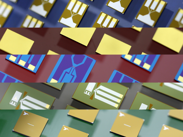
Our microfabrication division produces specialized chips in support of a wide range of in-situ microscopy applications. Examples are the following chip types:
- Window chips (multiple window geometries are available)
- Spacer chips (multiple thickness options are available)
- Electrochemistry chips (multiple electrode materials and geometries are available)
- Multiple-contact biasing chips
- Custom chips
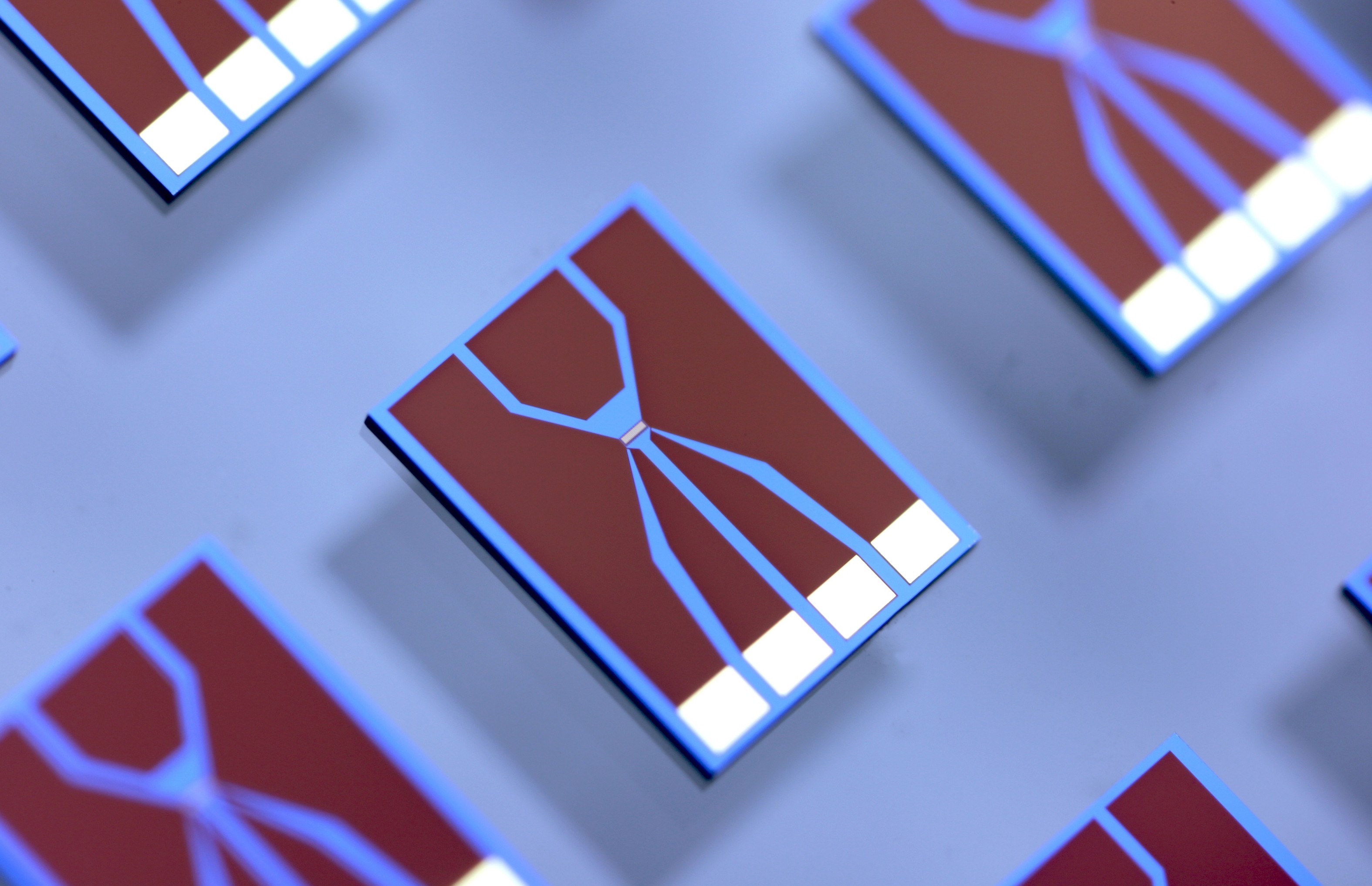
Different heater chips allow users to control temperature of the specimen in both liquid and gas environmental holders as well as the heating + biasing TEM holder. All our heater chips have closed loop temperature control using an on-chip sensor.
Temperature is a key environmental parameter in:
- Reactions of biological structures in liquid environments
- Kinetics and growth of nano-structures, line nano-articles and nano-wires.
- Corrosion
- Catalysis
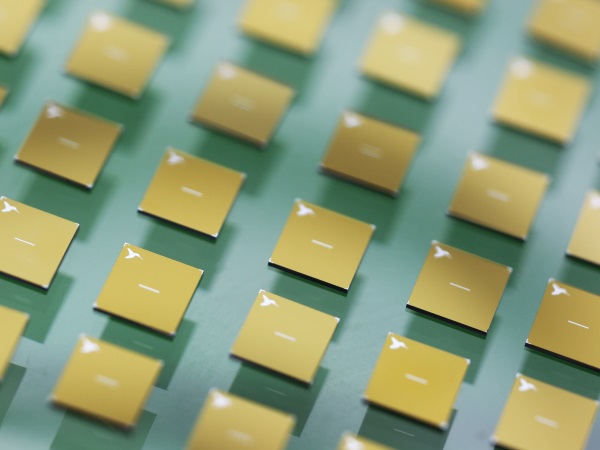
When stacked together and sealed by o-rings in the TEM, window and spacer chips enclose environmental conditions into an environmental cell. Environmental cells allow researchers to image specimens in-situ in the TEM inside a non-vacuum environment without extensive sample preparation.
The holders' features allow researchers to change the conditions within the cell during experiments and observe the influence on the specimen.
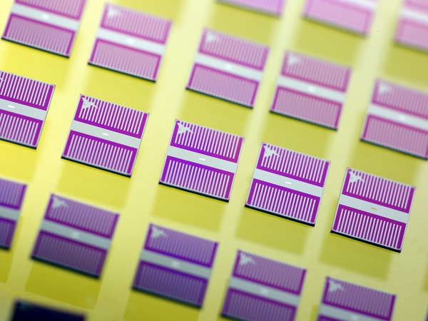
When stacked together and sealed by o-rings in the TEM, window and spacer chips enclose environmental conditions into an environmental cell. Environmental cells allow researchers to image specimens in-situ in the TEM inside a non-vacuum environment without extensive sample preparation.
Spacer chips are available in many thicknesses, allowing users to form liquid or gas flow channels specific to their needs. They can be paired with window chips, electrochemical chips, and heating chips to accommodate a variety of experimental designs.
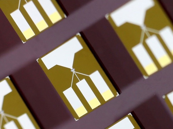
Hummingbird Scientific’s electrical biasing chips are developed specifically for our electrical biasing in-situ TEM holder and are available in a variety of electrode counts and materials. Electrical biasing holders allow scientists to operate small electrical devices in-situ in the TEM during imaging.
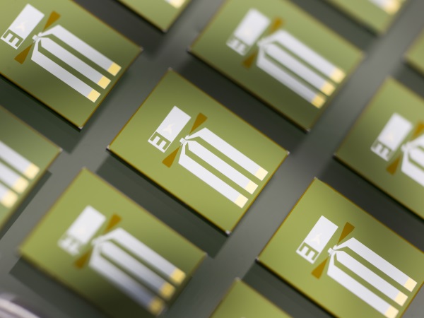
Electrochemical chips provide up to four electrical contacts inside the environmental cell, creating a complete electrochemical lab inside the TEM.
The chip's electrical leads are available in a large variety of electrochemical electrode patterns and materials.
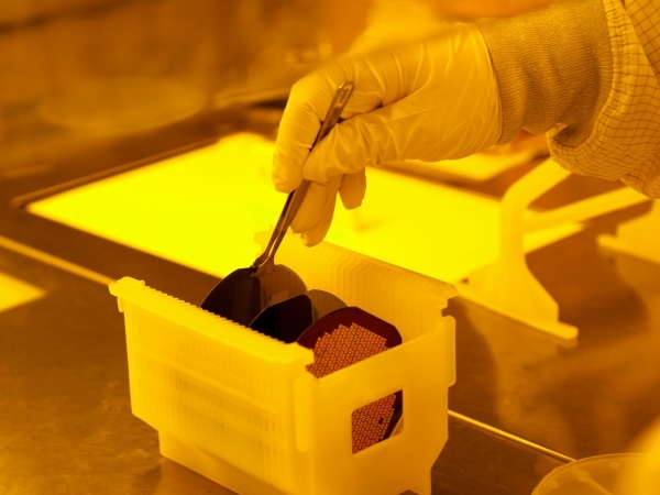
In addition to our standard biasing, liquid and gas cell chip products, the Microfabrication team at Hummingbird Scientific is excited to offer custom design and fabrication services to meet the unique needs of your experiment or process.
Our full service capabilities allow us to take a device design completely from concept to completion. We are eager to work with you, so let us know about your needs.
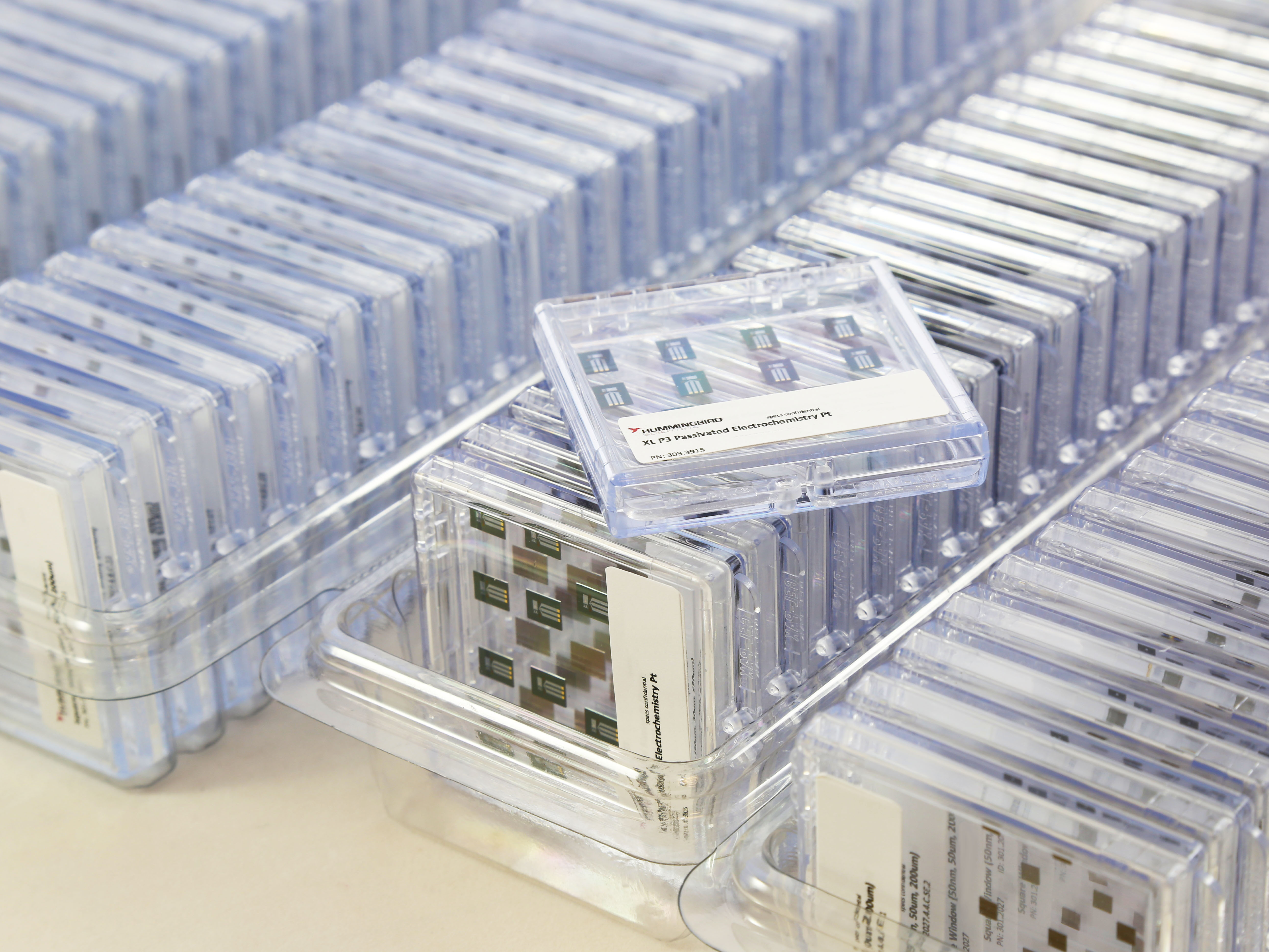
150,000+ chips produced
Hummingbird Scientific has produced well over 100,000 microfabricated chips for in situ microscopy and related advanced microscopy workflows.
That production history matters. Chip-based microscopy depends on repeatable fabrication, reliable inspection, clean handling, inventory availability, and compatibility with real holder and microscope systems. Hummingbird’s experience includes both standard chip production and hundreds of custom chip designs for specialized research and instrument-development programs.
This scale gives Hummingbird a deep practical understanding of how microfabricated chips perform in real experiments, not just how they look in design files.
Why in-house microfabrication matters
Microfabricated chips are central to many advanced microscopy experiments. They define the environment around the sample, provide electrical, thermal, fluidic, magnetic, or optical functions, and help determine whether an in situ experiment is stable, repeatable, and meaningful.
For Hummingbird Scientific, microfabrication is not a separate accessory business. It is part of the engineering system behind our in situ microscopy platforms. By connecting in-house microfabrication with product engineering, precision manufacturing, assembly, calibration, inspection, and microscope validation, Hummingbird can develop complete experimental systems rather than isolated parts.
That integration allows us to move from chip design to fabrication, inspection, testing, holder integration, and applications feedback within one development program.
Connected to our capabilities, facilities, and processes
Hummingbird’s in-house microfabrication capability is part of the company’s broader capabilities & facilities infrastructure. This connection is important because chip design, holder design, fluidic integration, electrical integration, heating performance, cryogenic workflows, and microscope validation are all connected in real experiments.
When a chip or device requires iteration, Hummingbird can connect microfabrication to engineering, manufacturing, assembly, calibration, inspection, software, and applications testing.
This shortens the feedback loop between design intent and experimental performance.
This is one reason Hummingbird can support advanced in situ microscopy systems, not only individual consumables.
Quality control, inspection, and packaging
Reliable chip performance requires more than fabrication. It requires inspection, cleaning, testing, packaging, handling practices, and compatibility with the holder or platform that will use the chip.
- Inspection at multiple stages of chip fabrication
- Micropatterning dimensional checks
- Cleaning procedures to reduce particle contamination
- Electrical testing for biasing and electrochemistry chips
- Heater calibration for heating chips
- Clean handling and sealed packaging until arrival at the user’s laboratory
- Training chips and best-practice handling support for users
This quality-control approach helps researchers get more reliable results from chip-based in situ microscopy experiments.
Reducing technical risk for grant-funded instrument development
In-house microfabrication reduces technical risk for NIH, SBIR, STTR, and other grant-funded instrument-development programs.
Grant-funded microscopy technology development often depends on the ability to move quickly from concept to prototype, from prototype to tested device, and from test results back to improved design. Hummingbird’s microfabrication capability supports this process directly.
- Design and fabricate prototype chips for new microscopy workflows
- Develop custom masks, electrode layouts, window geometries, and material stacks
- Inspect and test devices before integration
- Evaluate chip performance inside real holder and microscope workflows
- Iterate designs based on experimental feedback
- Support preliminary data generation and program execution
For reviewers and research partners, this capability helps demonstrate that Hummingbird has the internal infrastructure needed to execute chip-based microscopy development programs.
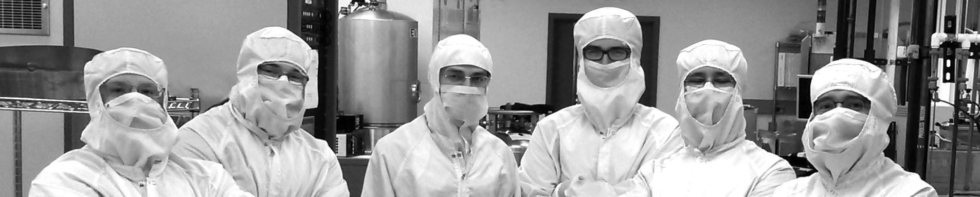
Microfabrication capabilities for in situ microscopy chips
Hummingbird’s in-house microfabrication capability supports the full development path for chip-based in situ microscopy devices, from design and mask layout through fabrication, inspection, testing, packaging, and integration with Hummingbird holders and custom platforms. This work supports standard chip production as well as custom microfabricated devices for TEM, SEM, X-ray microscopy, cryogenic workflows, and OEM instrument development.
Microfabrication process capabilities
Hummingbird supports both standard chip production and custom device development through a coordinated set of microfabrication, inspection, testing, and packaging capabilities, including:
- Custom mask design
- Photolithography
- Thin-film deposition
- Metal patterning
- Electrode patterning
- Dielectric layers
- Silicon nitride membrane and window fabrication
- Spacer fabrication
- Wafer bonding
- Wafer dicing
- Cleaning and packaging
- Optical inspection
- Electrical testing
- Heater calibration
Materials and custom material stacks
Hummingbird produces chips using a range of materials selected for microscopy compatibility, device function, and experimental requirements.
- Silicon
- Silicon nitride
- Silicon dioxide
- Gold
- Platinum
- Titanium
- Carbon
- Tungsten
- Aluminum oxide / alumina
- Glass
- Ceramics
- Copper
- Nickel
- Chromium
Custom material-stack designs can also be developed for specialized research, OEM, and platform-development programs.
Applications supported by Hummingbird microfabrication
Hummingbird microfabricated chips support a broad range of in situ and advanced microscopy workflows.
- Liquid cell TEM
- Gas cell TEM
- In situ heating
- Biasing and electrical testing
- Electrochemistry
- Battery research
- Catalysis
- Corrosion
- Semiconductor materials research
- Nanomaterials research
- X-ray microscopy
- SEM liquid flow
- Fast Freezing sample-preparation development
- Cryo-EM workflow development
- OEM and custom instrument development
Because these applications often require different window geometries, spacer thicknesses, electrode layouts, materials, thermal behavior, fluidic paths, or mechanical interfaces, microfabrication is directly connected to the success of the full experimental workflow.
Need standard chips, custom microfabricated devices, or an OEM microfabrication partner?
Hummingbird Scientific supports standard chip ordering, custom chip development, grant-funded instrument programs, and OEM/private-label platform development.
Hummingbird maintains standard chip inventory to help researchers keep experiments moving. Users can browse standard chips by holder, function, or application through the Hummingbird webstore.
- Browse standard chip varieties
- Order chips by holder or application
- Access available inventory
- Ship standard chips globally within 24 hours when available
- Contact Hummingbird or visit the Custom Solutions page linked below for custom chip geometries, materials, and device designs
For specialized projects, custom chip development is available.
Frequently asked questions
Our other capabilities and facilities
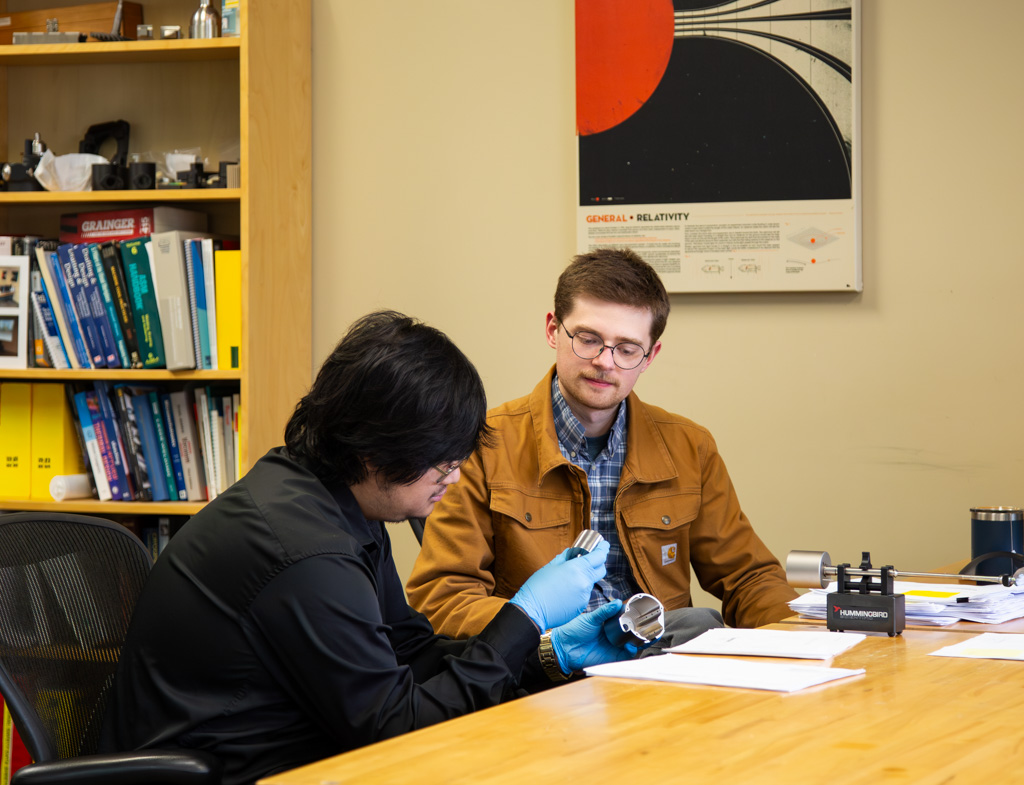
Engineering
From first-principles analysis and 3D CAD to prototyping, testing, and validation, see how Hummingbird develops advanced microscopy systems through integrated engineering, software, electronics, and manufacturing.
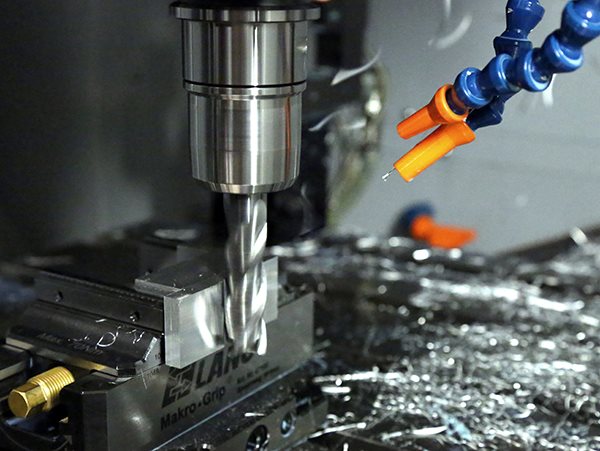
Manufacturing and Assembly
Our precision machine shop is the foundation of our in-house manufacturing, producing high-tolerance components for in situ microscopy. Paired with dedicated assembly and inspection, it ensures every part meets exacting performance and quality standards.

Calibration and inspection lab
In our in-house Calibration Lab, we measure thermal, electrical, and magnetic performance to ensure stable, accurate readouts that you can rely on from the start of every experiment.
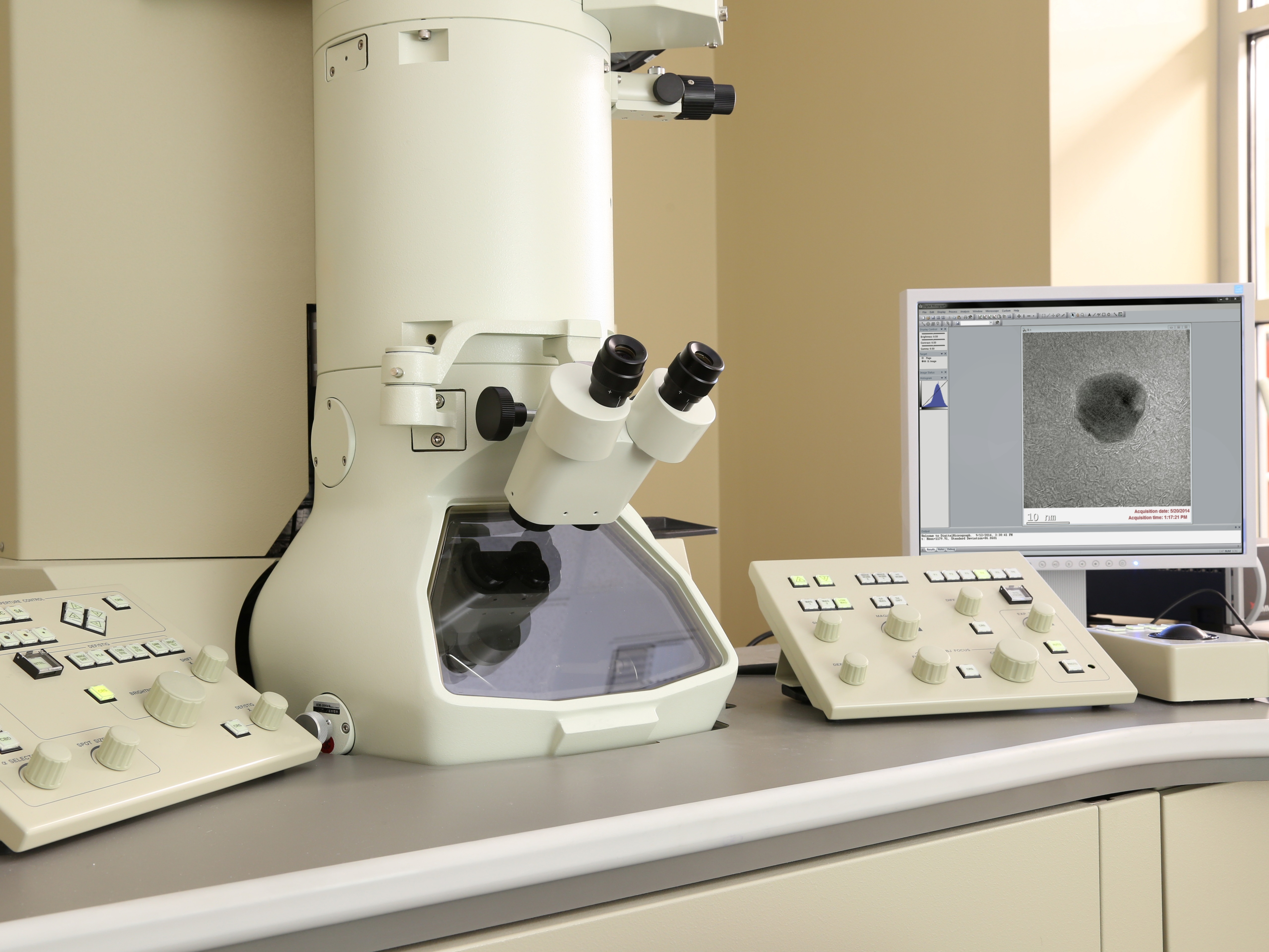
TEM and cryo-EM labs on site
Hummingbird maintains internal TEM and cryo-EM laboratories where products, prototypes, and workflows are developed and validated under real microscope conditions, connecting engineering decisions with practical performance and application needs.