Could real-time insight change how you design electrical materials and devices?
Hummingbird Scientific in-situ sample holders enable real-time characterization of electronic materials and devices at resolutions up to the atomic scale, linking structure directly to device performance. Conduct multimodal TEM, SEM, and X-ray experiments under applied bias, with closed-loop temperature control from −170 °C to above 1000 °C, to investigate switching behavior, interfacial dynamics, and nanoscale failure mechanisms.
Every Hummingbird holder is developed for performance, reproducibility, and ease of use. Scroll down to explore the types of experiments with electrical materials and devices made possible by these holders.

Which type of experiment best matches your research?
Electrical switching behavior
Directly observe electrical switching mechanisms and ionic transport in operating electronic devices.

Electrical switching behavior
Imaging reversible field-driven ionic transfer in bilayer switching devices
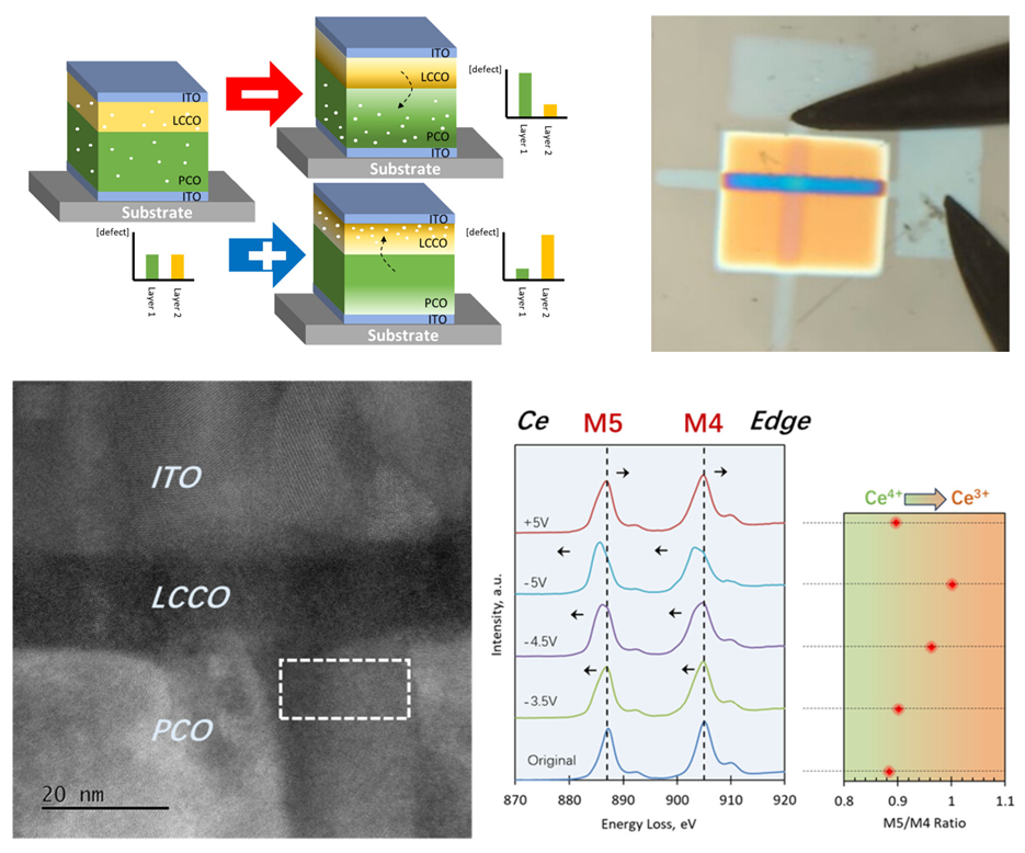
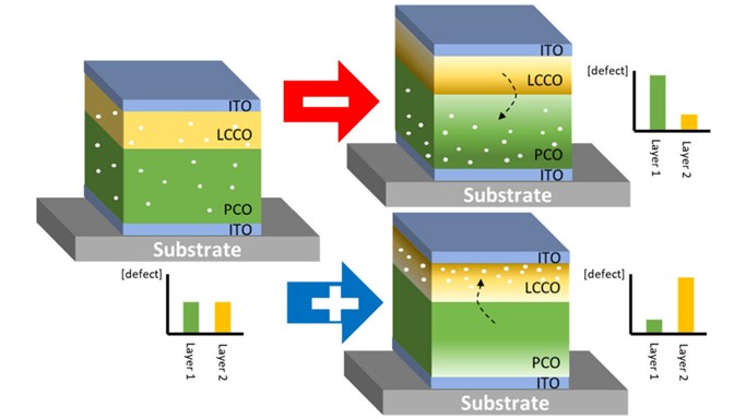
Reversible, field-driven modulation of electrical properties in Pr₀.₁Ce₀.₉O₂/La₁.₈₅Ce₀.₁₅CuO₄ (PCO/LCCO) thin-film bilayers was controlled and directly imaged in situ, revealing ionic transfer between the two solid oxide layers.
- Voltage-driven oxygen ion redistribution was achieved with high control and reversibility near ambient temperatures, spanning a wide range of oxygen activities.
- Systematic variation of defect concentrations enabled direct correlation with each film’s conductance.
- The study presents a more systematic approach for probing solid-solid exchange process in electrochemically controlled microelectronic devices.
Reference: Thomas Defferriere, et al, ACS Appl. Mater. Interfaces 16, 35, 46461-46472 (2024) DOI: 10.1021/acsami.4c09826
Image copyright © 2024 American Chemical Society

Operando electron holography
Visualize electric fields and charge distributions during electrical biasing of electronic materials and devices.
Operando electron holography
Mapping electric fields and imaging ferroelectric domain switching in hafnia-zirconia devices
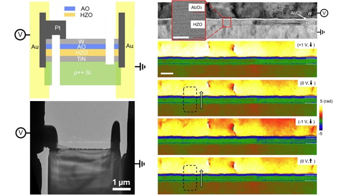
Internal electric fields within ferroelectric Hf0.5Zr0.5O2 /Al2O3 tunnel junctions were measured using in situ electrical biasing electron holography.
- Charge densities at internal interfaces were quantitatively determined.
- Polarization switching upon increasing voltage was revealed to occur via both the nucleation and lateral growth of domains.
- The approach is complementary to existing characterization techniques like HAADF and iDPC and opens new avenues for engineering the interfaces in ferroelectric devices.
Reference: Leifeng Zhang, et al, Nat Commun 16, 11233 (2025) DOI: 10.1038/s41467-025-66807-4
Image copyright © 2025, The Author(s). Published by Springer Nature Limited. This article is licensed under CC-BY 4.0.

2D materials-based devices
Investigate charge transport and electrical switching in operating 2D materials-based electronic devices.
2D materials-based devices
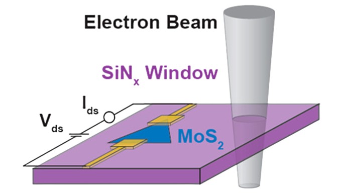
In-Situ TEM of an electron beam gated 2D MoS2 field-effect transistor
Electrical gating of 2D MoS2 channels was achieved using the TEM electron beam during operando biasing measurements.
- Electron-beam irradiation of the supporting SiNx membrane induced surface charging, reducing MoS₂ conductance by up to 94%.
- The effect was reversible, with on/off ratios reaching 56 at higher beam currents.
- The results demonstrate beam-induced substrate charging as a controllable gate for in situ study of 2D nanoelectronics devices without complex fabrication.
Reference: Paul Masih Das & Marija Drndić, ACS Nano 14, 6, 7389-7397 (2020). DOI: 10.1021/acsnano.0c02908
Image copyright © 2020 American Chemical Society

Electron beam-induced current (EBIC) imaging
Map electrical connectivity and electric fields in operating electronic devices.
Electron beam-induced current (EBIC) imaging
EBIC imaging of a hafnium zirconium oxide (Hf0.5Zr0.5O2, HZO) capacitor
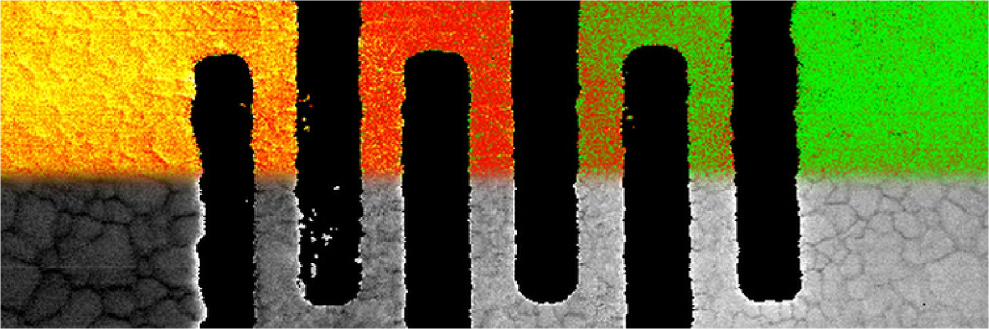
In situ STEM EBIC imaging of TaN/HZO/TaN capacitors was performed to map local polarization and directly correlate electrical switching with nanoscale domain behavior.
- Global polarization was measured using the positive-up, negative-down (PUND) transport method.
- The capacitor polarized after PUND measurements was subsequently imaged by STEM EBIC.
- Coercive-field mapping reveals individual domains to be biased “positive” and “negative”, instead of being “easy’ and “hard” to switch.
- The work establishes STEM EBIC as a revolutionary tool for characterizing ferroelectric materials and devices.
Reference: Ho Leung Chan, et al, ACS Nano 18, 31, 20380-20388 (2024). DOI: 10.1021/acsnano.4c04526
Image copyright © 2024, The Author(s). Published by American Chemical Society. This article is licensed under CC-BY 4.0.

Site-specific probing and biasing
Make precise localized electrical contacts and perform site-specific electrical measurements on electronic materials and devices.
Site-specific probing and biasing
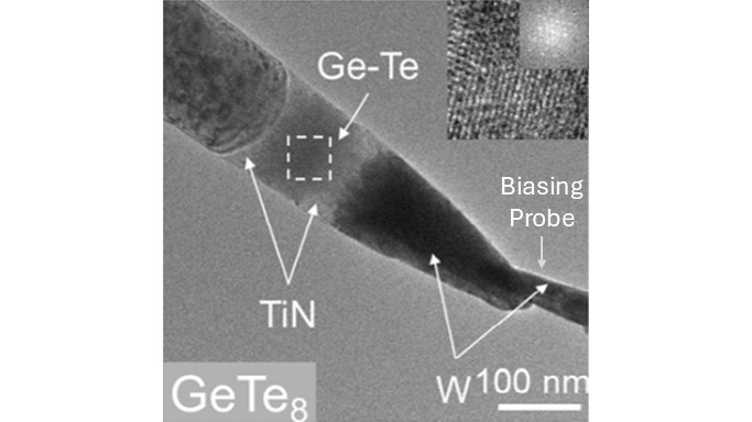
Electrical switching in Ge-Te devices via site-specific probing and biasing
In situ observations revealed the nanoscale structural rearrangements, phase transitions, and electrically driven switching pathways that governed volatile-to-non-volatile behavior in Ge–Te devices.
- Devices with different ratios of Ge v/s Te were tested for electrical switching behavior.
- Te rich materials switched via melting and recrystallization; mid-range compositions switched electronically only.
- Ge rich materials switched via amorphous to crystalline transformations.
- Demonstrates the advantages of site-specific biasing in nanodevice probing and testing.
Reference: Zihao Zhao, et al, ACS Nano 35, 23, 2423940 (2025). DOI: 10.1002/adfm.202423940
Image copyright © 2025 Wiley-VCH GmbH.

In-situ plasmon energy expansion thermometry
Measure nanoscale temperature distributions in electrically biased electronic materials and devices.
In-situ plasmon energy expansion thermometry
In-situ testing of nanoscale thermoelectric coolers
Cooling performance of single-crystal bismuth telluride (Bi2Te3) and antimony/bismuth telluride (Sb2–xBixTe3) based thermoelectric coolers was evaluated using plasmon energy expansion thermometry (PEET) and condensation thermometry.
- Structural characterization using STEM, SEM, and EDS; electrical characterization using STEM EBIC.
- In-situ PEET reveals Peltier cooling, up to ~21K below ambient, at low currents, which gets overtaken by Joule heating at higher currents.
- Condensation thermometry showed droplet formation in less than 0.5 seconds.
- Demonstrates the utility of in-situ thermometry for developing improved coolers.
Reference: William A. Hubbard, et al, ACS Nano 14, 9, 11510-11517 (2020). DOI: 10.1021/acsnano.0c03958
Image copyright © 2020 American Chemical Society
Electrical switching behavior
Directly observe electrical switching mechanisms and ionic transport in operating electronic devices.
Operando electron holography
Visualize electric fields and charge distributions during electrical biasing of electronic materials and devices.
2D materials-based devices
Investigate charge transport and electrical switching in operating 2D materials-based electronic devices.
%20imaging_thumbnail.jpg)
Electron beam-induced current (EBIC) imaging
Map electrical connectivity and electric fields in operating electronic devices.
Site-specific probing and biasing
Make precise localized electrical contacts and perform site-specific electrical measurements on electronic materials and devices.

In-situ plasmon energy expansion thermometry
Measure nanoscale temperature distributions in electrically biased electronic materials and devices.
Browse publications
Advanced Functional Materials
Nanotechnology
Nature Communications
Microscopy and Microanalysis
Research Spotlight
A microfabricated TaN/HZO/TaN capacitor is switched between the lower and upper signal paths for EBIC measurements. The positive-up-negative-down (PUND) sequence applied leaves the HZO polarized down. Subsequent EBIC imaging maps the remnant ⟨Er⟩, which nominally points up. Electron–hole pair separation produces a hole current (bright contrast) and an electron current (dark contrast). STEM images are acquired simultaneously. Video shows device-scale polarization data and domain-scale imaging of polarization and contrast switching with inset schematic of device and experimental setup.
Ferroelectric polarization imaged at nanoscale using electron beam-induced current
Typical STEM characterization and analysis reveal structural, mass-thickness, diffraction, and elemental composition information about nanoscale devices and semiconductor materials. EBIC techniques enable measurement of electronic properties such as conductivity and ferroelectric polarization. In this video, STEM-EBIC is used to image the ferroelectric polarization of an Hf₀.₅Zr₀.₅O₂ (HZO) capacitor, producing interpretable contrast that is linearly related to the measured ferroelectric polarization. Different combinations of EBIC signals generate unique image contrast, providing additional insight into domain behavior. Because the STEM-EBIC signal generated within the microfabricated capacitor varies linearly with the applied voltage, the resulting image can be interpreted as a map of the internal electric field.
Hummingbird Advantage
- Magnification-independent, tunable contrast for imaging ferroelectric polarization
- Low-noise, low-latency electronics provide rapid current contrast response
- Directly apply pulsed polarization voltages during STEM-EBIC experiments
- Measure remnant electric fields from polarized domains in the absence of an applied field
Reference: Ho Leung Chan, et al, ACS Nano (2024). DOI: 10.1021/acsnano.4c04526
Video Copyright © 2024 The Authors. Published by American Chemical Society. This publication is licensed under CC-BY 4.0.
Why choose Hummingbird Scientific for your research?
Hummingbird Scientific supports in situ electronics research with flexible microscopy platforms, customizable sample chips, direct scientist support, internal TEM lab expertise, and in-house engineering and manufacturing capabilities.
Broader options for in situ electronics experiments
Electronics experiments span electrical biasing, thermal stressing, cryogenic characterization, nanoprobing, failure analysis, and multimodal correlative workflows. Hummingbird supports these studies with in situ TEM, SEM, and X-ray microscopy platforms offering electrical biasing, heating, cooling, nano-manipulation, and environmental experiment configurations. This gives researchers the flexibility to match the experimental platform to the device architecture, operating conditions, and measurement objectives.
More chip choices for experimental flexibility
Microfabricated chip design plays a critical role in electronics characterization. Through our dedicated microfabrication division, Hummingbird supports standard and custom chips for electrical biasing, heating, and combined heating + biasing, with configurable window geometries and electrode layouts. This flexibility allows researchers to optimize chip designs for specific devices, materials, and experimental workflows while maintaining compatibility across multiple microscopy platforms.
Scientist support backed by an internal TEM Lab
Electronics researchers work directly with scientists and technical staff who understand the practical details of in situ and operando TEM workflows. Hummingbird’s internal TEM Lab allows our team to evaluate microscope-facing performance during development, including alignment, handling, imaging stability, sample-environment behavior, and workflow usability under real TEM conditions.
Engineering, production, and custom capability
Hummingbird's in-house capabilities connect engineering, microfabrication, manufacturing, assembly, calibration, and testing within one development process. For electronics research, that means standard products can be supported by custom chips and holder configurations, and application-specific workflow changes when the experiment requires something more specific.
Electrical switching behavior
Directly observe electrical switching mechanisms and ionic transport in operating electronic devices.
Electrical switching behavior
Imaging reversible field-driven ionic transfer in bilayer switching devices
Reversible, field-driven modulation of electrical properties in Pr₀.₁Ce₀.₉O₂/La₁.₈₅Ce₀.₁₅CuO₄ (PCO/LCCO) thin-film bilayers was controlled and directly imaged in situ, revealing ionic transfer between the two solid oxide layers.
- Voltage-driven oxygen ion redistribution was achieved with high control and reversibility near ambient temperatures, spanning a wide range of oxygen activities.
- Systematic variation of defect concentrations enabled direct correlation with each film’s conductance.
- The study presents a more systematic approach for probing solid-solid exchange process in electrochemically controlled microelectronic devices.
Reference: Thomas Defferriere, et al, ACS Appl. Mater. Interfaces 16, 35, 46461-46472 (2024) DOI: 10.1021/acsami.4c09826
Image copyright © 2024 American Chemical Society
Operando electron holography
Visualize electric fields and charge distributions during electrical biasing of electronic materials and devices.
Operando electron holography
Mapping electric fields and imaging ferroelectric domain switching in hafnia-zirconia devices
Internal electric fields within ferroelectric Hf0.5Zr0.5O2 /Al2O3 tunnel junctions were measured using in situ electrical biasing electron holography.
- Charge densities at internal interfaces were quantitatively determined.
- Polarization switching upon increasing voltage was revealed to occur via both the nucleation and lateral growth of domains.
- The approach is complementary to existing characterization techniques like HAADF and iDPC and opens new avenues for engineering the interfaces in ferroelectric devices.
Reference: Leifeng Zhang, et al, Nat Commun 16, 11233 (2025) DOI: 10.1038/s41467-025-66807-4
Image copyright © 2025, The Author(s). Published by Springer Nature Limited. This article is licensed under CC-BY 4.0.
2D materials-based devices
Investigate charge transport and electrical switching in operating 2D materials-based electronic devices.
2D materials-based devices
In-Situ TEM of an electron beam gated 2D MoS2 field-effect transistor
Electrical gating of 2D MoS2 channels was achieved using the TEM electron beam during operando biasing measurements.
- Electron-beam irradiation of the supporting SiNx membrane induced surface charging, reducing MoS₂ conductance by up to 94%.
- The effect was reversible, with on/off ratios reaching 56 at higher beam currents.
- The results demonstrate beam-induced substrate charging as a controllable gate for in situ study of 2D nanoelectronics devices without complex fabrication.
Reference: Paul Masih Das & Marija Drndić, ACS Nano 14, 6, 7389-7397 (2020). DOI: 10.1021/acsnano.0c02908
Image copyright © 2020 American Chemical Society
Electron beam-induced current (EBIC) imaging
Map electrical connectivity and electric fields in operating electronic devices.
Electron beam-induced current (EBIC) imaging
EBIC imaging of a hafnium zirconium oxide (Hf0.5Zr0.5O2, HZO) capacitor
In situ STEM EBIC imaging of TaN/HZO/TaN capacitors was performed to map local polarization and directly correlate electrical switching with nanoscale domain behavior.
- Global polarization was measured using the positive-up, negative-down (PUND) transport method.
- The capacitor polarized after PUND measurements was subsequently imaged by STEM EBIC.
- Coercive-field mapping reveals individual domains to be biased “positive” and “negative”, instead of being “easy’ and “hard” to switch.
- The work establishes STEM EBIC as a revolutionary tool for characterizing ferroelectric materials and devices.
Reference: Ho Leung Chan, et al, ACS Nano 18, 31, 20380-20388 (2024). DOI: 10.1021/acsnano.4c04526
Image copyright © 2024, The Author(s). Published by American Chemical Society. This article is licensed under CC-BY 4.0.
Site-specific probing and biasing
Make precise localized electrical contacts and perform site-specific electrical measurements on electronic materials and devices.
Site-specific probing and biasing
Electrical switching in Ge-Te devices via site-specific probing and biasing
In situ observations revealed the nanoscale structural rearrangements, phase transitions, and electrically driven switching pathways that governed volatile-to-non-volatile behavior in Ge–Te devices.
- Devices with different ratios of Ge v/s Te were tested for electrical switching behavior.
- Te rich materials switched via melting and recrystallization; mid-range compositions switched electronically only.
- Ge rich materials switched via amorphous to crystalline transformations.
- Demonstrates the advantages of site-specific biasing in nanodevice probing and testing.
Reference: Zihao Zhao, et al, ACS Nano 35, 23, 2423940 (2025). DOI: 10.1002/adfm.202423940
Image copyright © 2025 Wiley-VCH GmbH.
In-situ plasmon energy expansion thermometry
Measure nanoscale temperature distributions in electrically biased electronic materials and devices.
In-situ plasmon energy expansion thermometry
In-situ testing of nanoscale thermoelectric coolers
Cooling performance of single-crystal bismuth telluride (Bi2Te3) and antimony/bismuth telluride (Sb2–xBixTe3) based thermoelectric coolers was evaluated using plasmon energy expansion thermometry (PEET) and condensation thermometry.
- Structural characterization using STEM, SEM, and EDS; electrical characterization using STEM EBIC.
- In-situ PEET reveals Peltier cooling, up to ~21K below ambient, at low currents, which gets overtaken by Joule heating at higher currents.
- Condensation thermometry showed droplet formation in less than 0.5 seconds.
- Demonstrates the utility of in-situ thermometry for developing improved coolers.
Reference: William A. Hubbard, et al, ACS Nano 14, 9, 11510-11517 (2020). DOI: 10.1021/acsnano.0c03958
Image copyright © 2020 American Chemical Society
Featured products


Frequently asked questions
Ready to discuss your experiment?
Talk with an applications scientist to identify the right products for your experiment and request a quote.