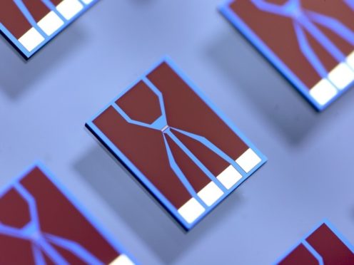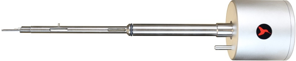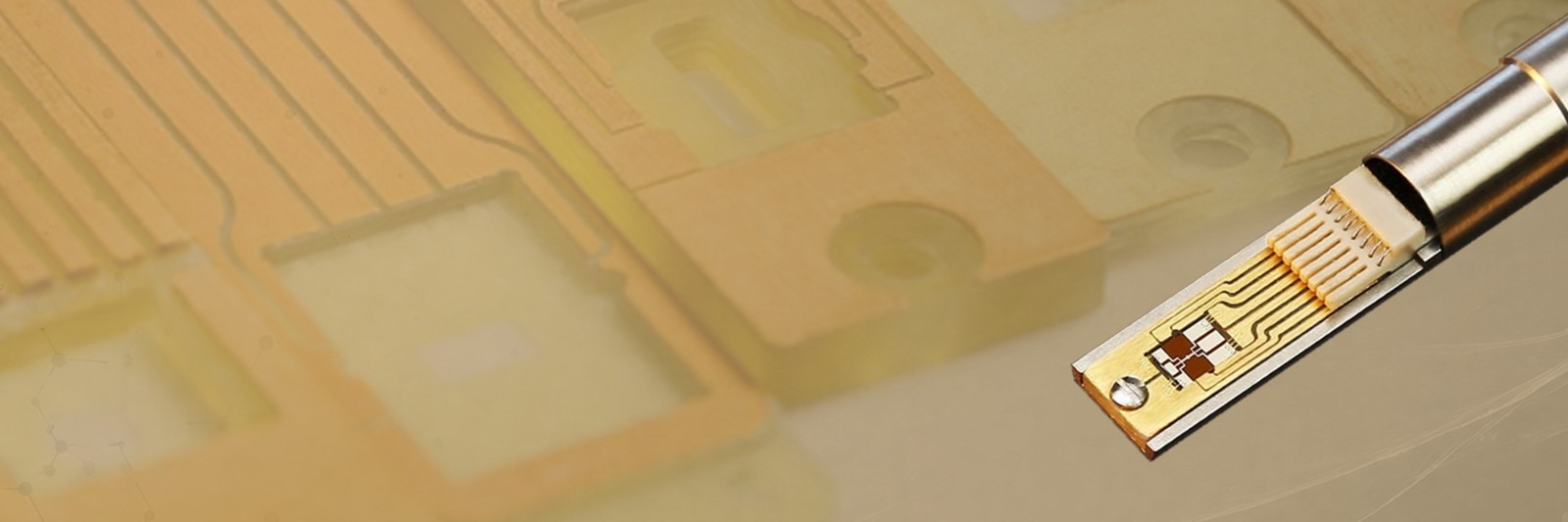
Expand your in-situ TEM electrical biasing capabilities with a flexible platform that supports both Hummingbird Scientific chips and user-developed devices through custom chip-carrier geometries
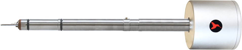
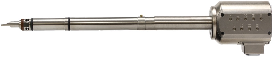
The Hummingbird Scientific TEM Electrical Biasing: Flexible Carrier Sample Holder enables in-situ electrical biasing using Hummingbird Scientific MEMS chips, user-developed devices, and custom sample carriers within a single adaptable platform. Designed for researchers in semiconductor devices, energy storage, quantum materials, nanotechnology, electronics, and materials science, it supports investigations of electrical transport, device performance, electrochemical reactions, phase transformations, and failure mechanisms across a wide range of sample formats. By correlating electrical stimuli with atomic-resolution imaging and analytical characterization, researchers can reveal the mechanisms governing material behavior and device performance without being limited to a single chip architecture.
Hummingbird Advantages:
- Compatible with Hummingbird Scientific MEMS chips, user-developed devices, and custom sample carriers.
- Eight independent electrical contacts for simultaneous electrical biasing and electrical measurements.
- Individually shielded wiring minimizes electrical noise for sensitive electrical characterization.
- Full compatibility with TEM, STEM, EDS, and EELS during electrical biasing experiments.
- Choose from multiple chip geometries and materials manufactured through Hummingbird Scientific's in-house microfabrication facility.
- Expand experimental capabilities with custom carrier and MEMS chip development tailored to your research.
Available For:




.jpg)

How it Works
Hummingbird Scientific electrical biasing chips, user-developed chips, and custom devices are wire bonded to interchangeable chip carriers before being inserted into the holder tip. Spring-loaded electrical contacts automatically establish reliable electrical connections, while individually shielded wiring minimizes electrical noise to support sensitive electrical measurements and repeatable experimental performance.
During in-situ TEM experiments, electrical stimuli are applied while structural, morphological, and chemical changes are observed using conventional TEM imaging together with analytical techniques such as EDS and EELS. The platform supports a broad range of electrical characterization workflows, from routine device testing to advanced operando materials research.
The interchangeable carrier architecture enables new chip designs, custom devices, and specialized sample geometries to be accommodated without changing the overall experimental platform. This flexible approach allows experimental capabilities to expand as research priorities, device architectures, and electrical characterization requirements evolve.
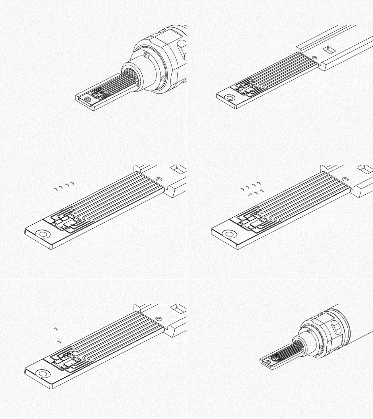
Key Features and Capabilities
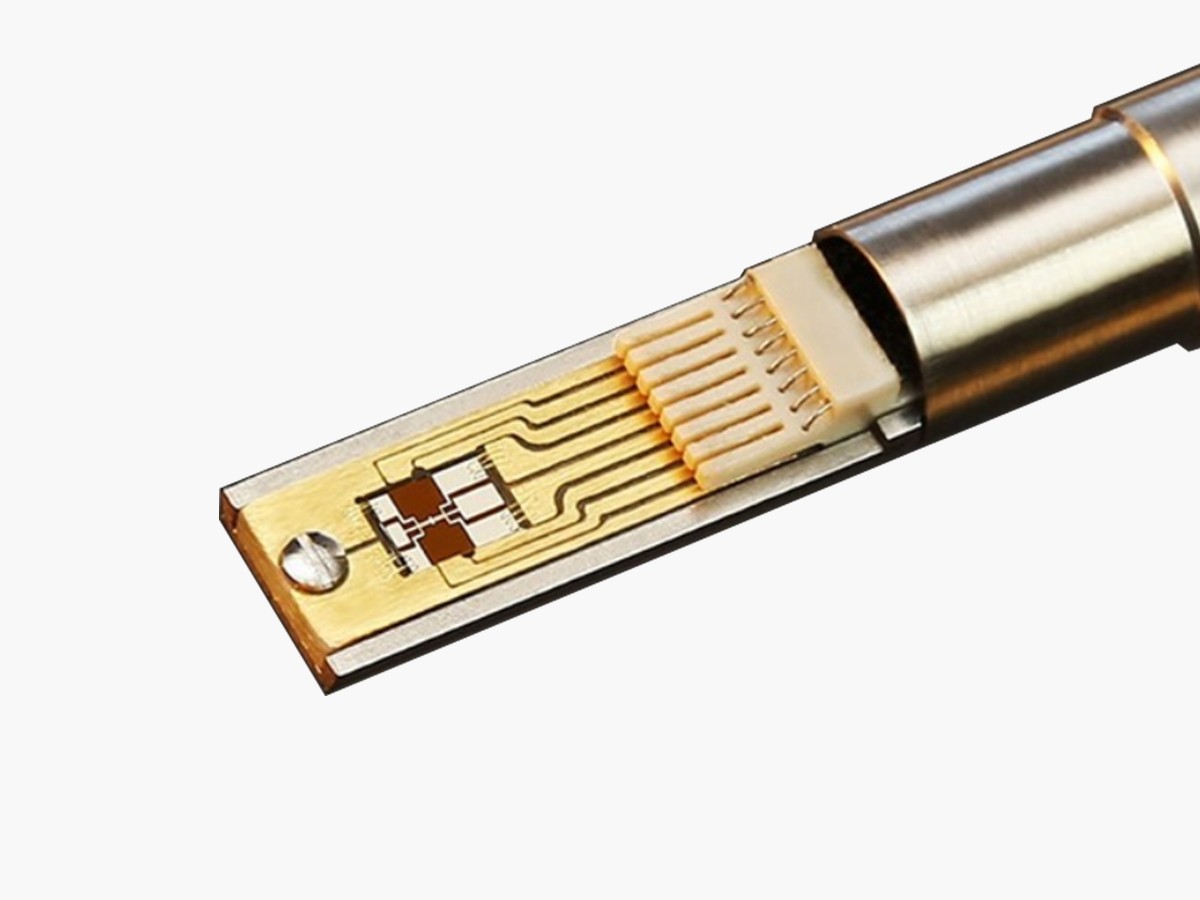
Support Hummingbird Scientific chips, user-developed chips, and custom devices on the same holder
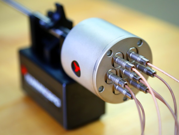
Perform sensitive electrical measurements through eight independently shielded electrical contacts
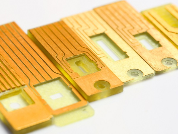
Expand experimental capabilities with application-specific carrier designs for unique devices and samples
Built for Diverse Research Applications

Featured Research
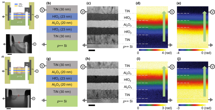
a,f) FIB lamellae schematic and TEM image of stack A: HfO2/Al2O3/HfO2 and stack B: Al2O3/HfO2/Al2O3. b,g) Sketches of stacks A and B. c,h) TEM images layers of the nanocapacitors A and B. d,i) Phase maps of projected electric potential obtained by electron holography for nanocapacitors A and B with an applied bias of +6 V. e,j) Phase maps for nanocapacitors A and B with an applied bias of -6 V. Scale bars are 20 nm in (c) and (h).
Operando electron holography of trapped charges in multilayer HfO₂–Al₂O₃ nanocapacitors
The Hummingbird Scientific TEM Electrical Biasing: Flexible Carrier sample holder enabled operando off-axis electron holography of multilayer HfO2/Al2O3 nanocapacitors during electrical biasing. Focused-ion beam lamellae supporting HfO2/Al2O3/HfO2 and Al2O3/HfO2/Al2O3 stacks were mounted across biasing microchip contacts, allowing electrostatic potential mapping at sub-nanometer spatial resolution while voltage was applied. The measurements directly quantified trapped charges at both dielectric/dielectric and metal/dielectric interfaces and revealed how these charges modify local electric field distributions within the devices. Operando holography demonstrated, for the first time, a linear relationship between interfacial trapped charge density and applied bias, providing new insight into the behavior of nanoscale electronic and memory devices.
Reference: Leifeng Zhang, et al. Advanced Materials (2025). DOI: 10.1002/adma.202413691
Copyright © 2024 The Author(s). Advanced Materialspublished by Wiley-VCH GmbH.
Video Spotlight
Spectrum image of well-developed SEI. ADF STEM image (top) is acquired simultaneously with the spectrum image (middle). The scanning dotted line on the spectra plot (bottom) indicates the 50 meV energy slice shown in the EELS image.
Operando EELS spectral imaging of the solid-electrolyte interphase in lithium-ion batteries
The Hummingbird Scientific TEM Electrical Biasing Flexible Carrier sample holder enabled operando STEM-EELS spectral imaging of the solid-electrolyte interphase (SEI) formed on graphite during lithium-ion battery cycling. The video highlights the active pixels of a fully developed SEI along at each 50 meV energy slice of the EELS spectral domain, mapping the chemical composition varies across dendrites, lithium-rich regions, lithium hydride deposits, and the surrounding SEI. The video highlights chemical transformations at liquid-solid interfaces during operando electrochemical biasing and in-situ spectroscopic mapping, revealing the multi-phase and heterogeneous chemical structure of the SEI with operando spectral imaging of a functioning battery environment.
Hummingbird Advantages
- Cell construction, battery cycling and SEI formation all without exposure to air
- Flexibly compatible with a wide variety of devices including DIY-battery microcells
- Versatile chips with a variety of electrode geometries optimized for battery cell construction
- Liquid thickness and sample stability suitable for EELS acquisition
Reference: Jared J. Lodico, et al. Science Advances (2023). DOI:10.1126/sciadv.adg5135
Video Copyright © 2023 The Authors. Publishedby the American Association for the Advancement of Science under the CreativeCommons Attribution License (CC BY).
Built on Engineering Excellence
Hummingbird Scientific designs, machines, assembles, tests, and services its products in-house. Our integrated in-house engineering, precision manufacturing, microfabrication, software development, applications, and service teams enable rapid prototyping and iteration, custom modifications, and direct technical support throughout the life of the instrument.
The TEM Electrical Biasing: Flexible Carrier Sample Holder combines precision holder mechanics with a flexible carrier architecture that accommodates standard Hummingbird Scientific electrical biasing chips as well as user-developed chips and custom devices. Multiple carrier geometries can be developed to support specialized sample layouts, electrical contact schemes, and emerging device architectures, providing the flexibility to adapt the platform to evolving research requirements.
Need something unique? Our engineers can customize existing products or develop new solutions to support specialized MEMS chip designs, electrical configurations, sample geometries, and emerging research challenges.
Frequently Asked Questions
Related Products


Customization and Service