Measure electronic properties using two independent Electron Beam-Induced Current (EBIC) channels while correlating electronic, structural, and chemical information from the same nanoscale region during TEM/STEM analysis.
The NEI Two-Channel STEM EBIC System enables simultaneous Electron Beam-Induced Current (EBIC), Secondary Electron Electron Beam-Induced Current (SEEBIC), and TEM/STEM analysis within a single experiment. Designed for researchers in semiconductor devices, nanoelectronics, quantum materials, and functional materials, it supports investigations of charge transport, electric fields, polarization, current pathways, device operation, and failure mechanisms. By correlating electronic measurements with atomic-resolution imaging and analytical characterization, researchers gain deeper insight into the relationships between electronic behavior, structure, and composition.
Hummingbird Advantages:
- Simultaneously acquire EBIC, SEEBIC, TEM/STEM, EDS, and EELS data from the same nanoscale region.
- Separate complementary Electron Beam-Induced Current (EBIC) and Secondary Electron Electron Beam-Induced Current (SEEBIC) signals using two independent measurement channels.
- Capture the most subtle nano-electronic contrast with current resolution in the 10s of fA.
- Measure subtle electronic responses with low-noise current acquisition and signal conditioning.
- Improve experiment reproducibility through reliable electrical contact and repeatable screw-free direct chip loading.
- Optional integrated heating enables temperature-dependent EBIC and SEEBIC measurements.
Available For:


.jpg)
How it Works
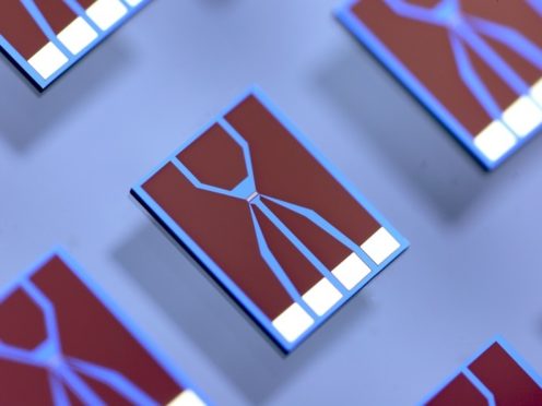
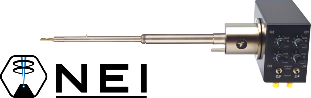
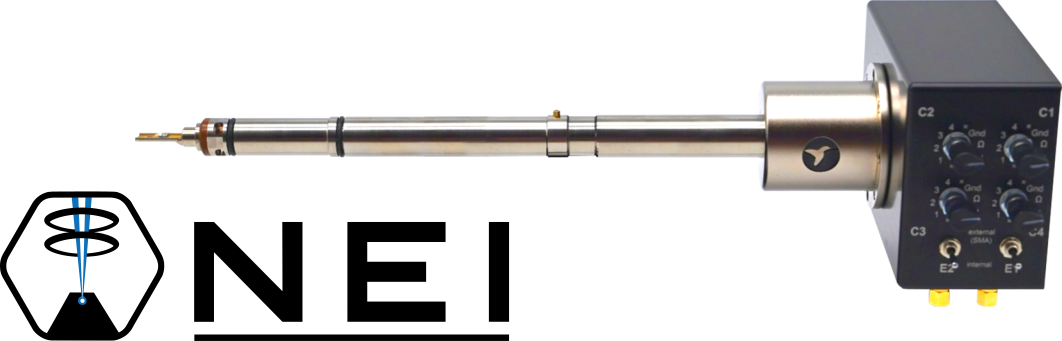
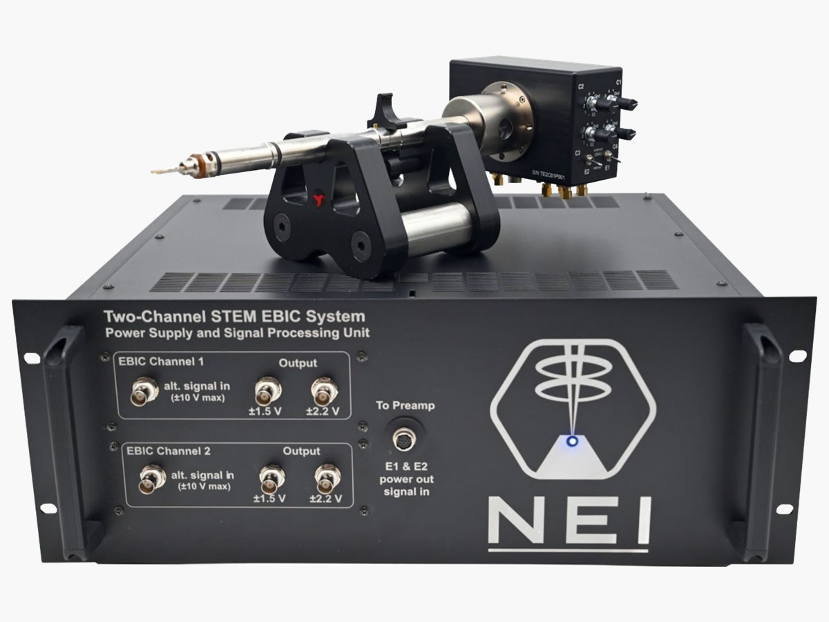
The NEI Two-Channel STEM EBIC System combines a Hummingbird Scientific TEM sample holder with NanoElectronic Imaging (NEI) low-noise Electron Beam-Induced Current (EBIC) electronics, compatible sample substrates, and signal conditioning hardware into a correlative electronic characterization workflow.
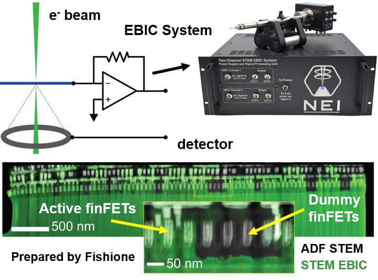
An electrically contacted sample is mounted on an EBIC-compatible substrate and inserted into the TEM for STEM imaging. As the focused electron probe scans the sample, beam-sample interactions generate Electron Beam-Induced Current (EBIC) and Secondary Electron Electron Beam-Induced Current (SEEBIC) signals. Two independent, low-noise current measurement channels acquire and synchronize these signals with probe position to generate spatially resolved current maps.
Correlate conductivity, charge transport, electric fields, polarization, and current pathways with TEM/STEM imaging, Energy-Dispersive X-ray Spectroscopy (EDS), and Electron Energy Loss Spectroscopy (EELS) from the same nanoscale region. Optional heating and double-tilt capabilities extend the workflow to temperature-dependent studies and precise crystal orientation for advanced electronic materials research.
Key Features and Capabilities
Acquire independent Electron Beam-Induced Current (EBIC) and Secondary Electron Electron Beam-Induced Current (SEEBIC) signals for correlative electronic characterization
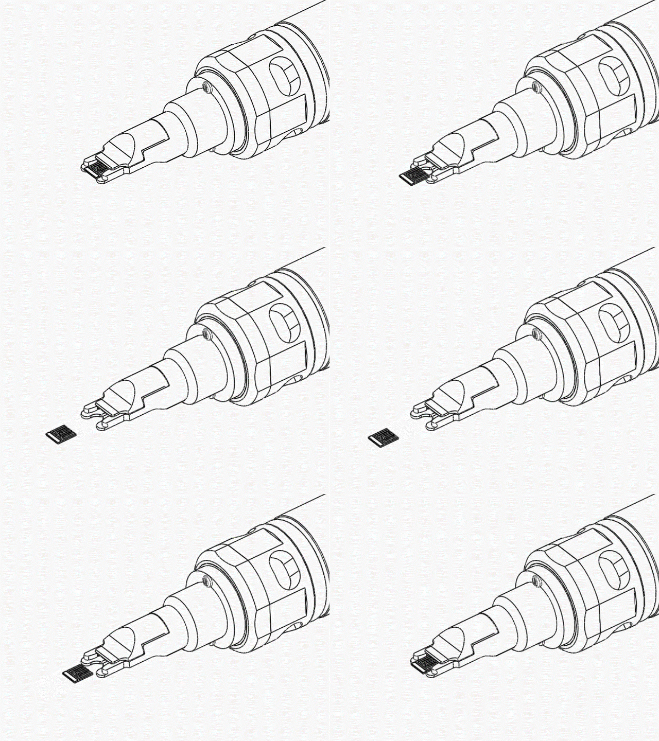
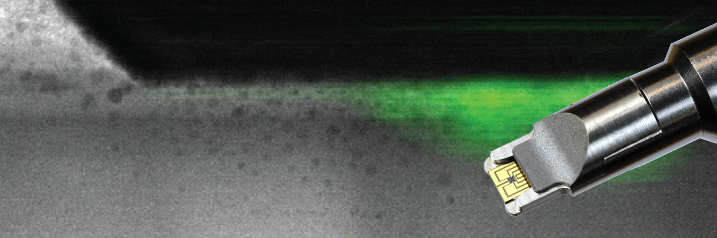
Load MEMS chips quickly with reliable electrical contact and simplified experiment setup
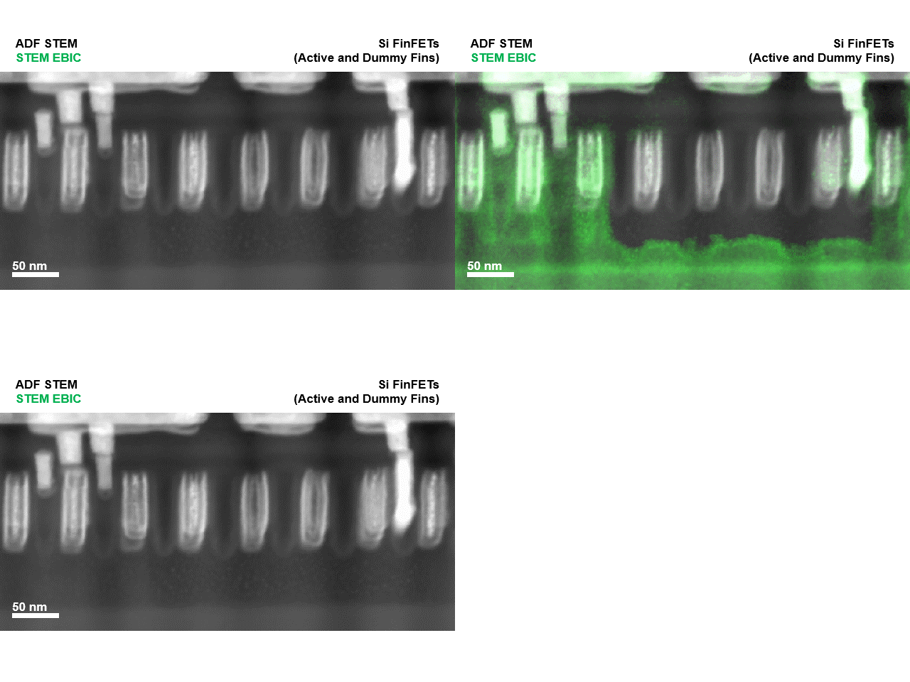
Relate electronic properties directly to crystal structure and chemical composition during a single experiment
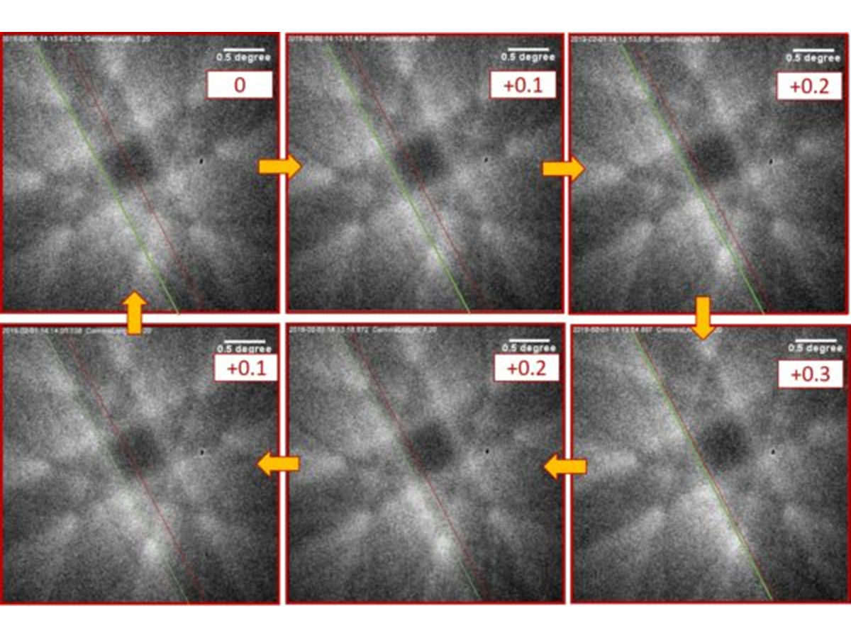
Optimize sample orientation for diffraction, crystallography, and analytical TEM workflows using the double-tilt holder configuration

Keep experiments moving with in-stock MEMS chips for in-situ TEM heating, electrical biasing, and STEM EBIC
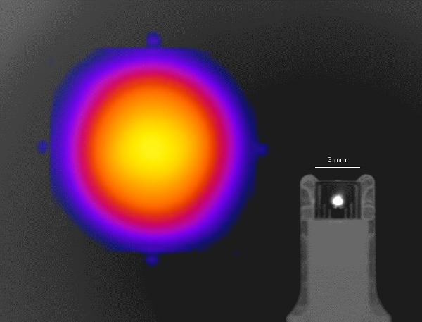
Study temperature-dependent electronic behavior while maintaining correlative TEM/STEM characterization
Built for Diverse Research Applications

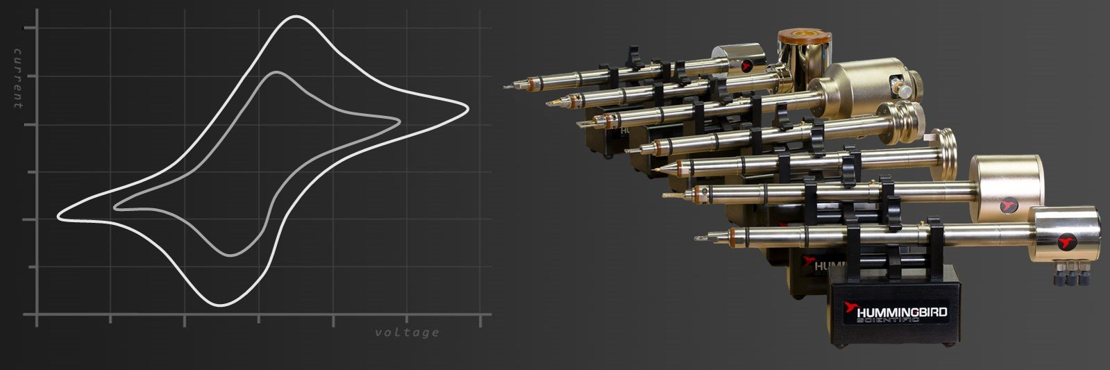
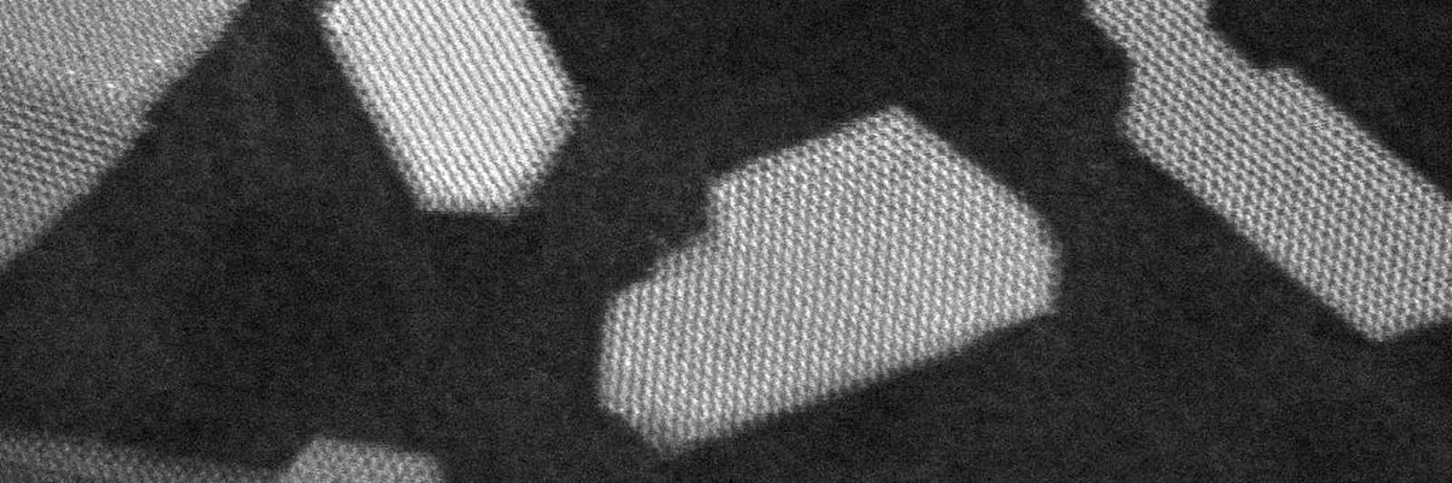
Featured Research
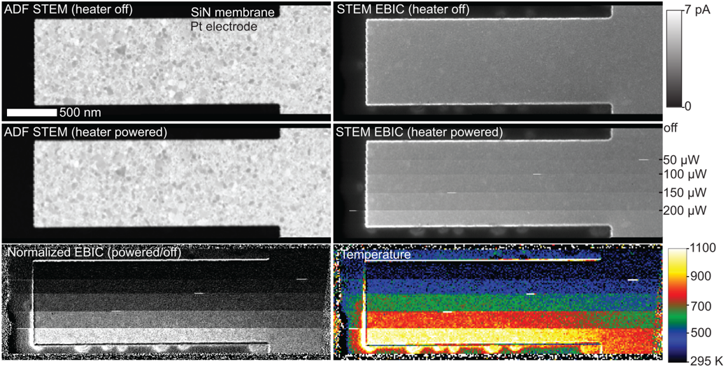
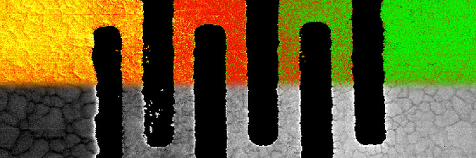
The ADF STEM and STEM EBIC images show an un-calibrated Pt heater-electrode structure. The device is shown with the heater off (top),and with the heater power increased during acquisition (middle). The heater-on image divided by the heater-off image generates a map of Θ(˜T) (lower-left), which when binned by two can be used to calculate the temperature map (lower-right).
Nanoscale thermometry using two-channel STEM-EBIC and secondary electron emission mapping
The Hummingbird Scientific/NEI Two-Channel STEM EBIC System was used to map temperature-dependent secondary electron emission currents with nanoscale spatial resolution in operating microfabricated devices. By acquiring STEM-EBIC signals simultaneously with conventional STEM imaging, the platform measured changes in secondary electron emission from platinum, amorphous carbon, and aluminum structures as they were heated in situ. Aluminum nanoparticle thermometers calibrated using plasmon energy expansion thermometry (PEET) provided local temperature references, enabling quantitative correlation between EBIC signal and temperature. The study demonstrated that secondary electron emission current mapping can produce quantitative temperature maps and offers a widely applicable approach to TEM-based nanoscale thermometry.
Reference: William A. Hubbard, et al. Nanotechnology (2025). DOI: 10.1088/1361-6528/ade445
Copyright © 2025 IOP Publishing Ltd. All rights reserved. Following the 12‑month embargo period, the accepted manuscript will be available under a CC BY‑NC‑ND 4.0 license.
Video Spotlight
A microfabricated TaN/HZO/TaN capacitor is switched between the lower and upper signal paths for EBIC measurements. The positive-up-negative-down (PUND) sequence applied leaves the HZO polarized down. Subsequent EBIC imaging maps the remnant ⟨Er⟩, which nominally points up. Electron–hole pair separation produces a hole current (bright contrast) and an electron current (dark contrast). STEM images are acquired simultaneously. Video shows device-scale polarization data and domain-scale imaging of polarization and contrast switching with inset schematic of device and experimental setup.
Ferroelectric polarization imaged at nanoscale using electron beam-induced current
Typical STEM characterization and analysis reveal structural, mass-thickness, diffraction, and elemental composition information about nanoscale devices and semiconductor materials. EBIC techniques enable measurement of electronic properties such as conductivity and ferroelectric polarization. In this video, STEM-EBIC is used to image the ferroelectric polarization of an Hf₀.₅Zr₀.₅O₂ (HZO) capacitor, producing interpretable contrast that is linearly related to the measured ferroelectric polarization. Different combinations of EBIC signals generate unique image contrast, providing additional insight into domain behavior. Because the STEM-EBIC signal generated within the microfabricated capacitor varies linearly with the applied voltage, the resulting image can be interpreted as a map of the internal electric field.
Hummingbird Advantage
- Magnification-independent, tunable contrast for imaging ferroelectric polarization
- Low-noise, low-latency electronics provide rapid current contrast response
- Directly apply pulsed polarization voltages during STEM-EBIC experiments
- Measure remnant electric fields from polarized domains in the absence of an applied field
Reference: Ho Leung Chan, et al, ACS Nano (2024). DOI: 10.1021/acsnano.4c04526
Video Copyright © 2024 The Authors. Published by American Chemical Society. This publication is licensed under CC-BY 4.0.
Software
Spend less time managing equipment and more time generating results. Hummingbird Control™ Software provides intuitive control of heating and biasing functions, including temperature set points, closed-loop heating behavior, and voltage sweep workflows when configured with the system.
Hummingbird Connect™ can support the broader software strategy by connecting holder operation, microscope context, imaging workflows, and experiment metadata. Together, these software tools help improve reproducibility, experiment setup, data organization, and long-term usability for your STEM EBIC experiments.
Built on Engineering Excellence
Hummingbird Scientific designs, machines, assembles, tests, and services its products in-house. Our integrated engineering, precision manufacturing, microfabrication, software development, and applications teams work together to develop specialized sample holders and experimental workflows that support advanced TEM, SEM, and X-ray microscopy. This vertically integrated approach enables rapid prototyping and iteration, custom modifications, and direct technical support while maintaining the precision and reliability required for demanding in-situ microscopy experiments.
The NEI Two-Channel STEM EBIC System is developed and produced by NanoElectronic Imaging (NEI), combining Hummingbird Scientific's TEM holder engineering with low-noise Electron Beam-Induced Current (EBIC) electronics developed by NEI. The integrated system provides reliable electrical connections, stable TEM operation, and compatibility with a broad range of sample substrates for semiconductor devices, functional materials, and nanoelectronic systems. Correlative acquisition of EBIC, Secondary Electron Electron Beam-Induced Current (SEEBIC), TEM/STEM imaging, Energy-Dispersive X-ray Spectroscopy (EDS), and Electron Energy Loss Spectroscopy (EELS) supports comprehensive characterization from the same nanoscale region.
Need something beyond a standard configuration? Hummingbird Scientific can modify existing holder designs, integrate specialized sample substrates, and develop custom experimental workflows to support emerging electronic materials research and application-specific requirements.
Frequently Asked Questions
Related Products


Customization and Service