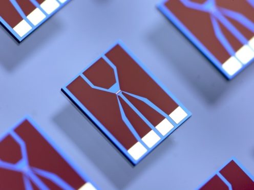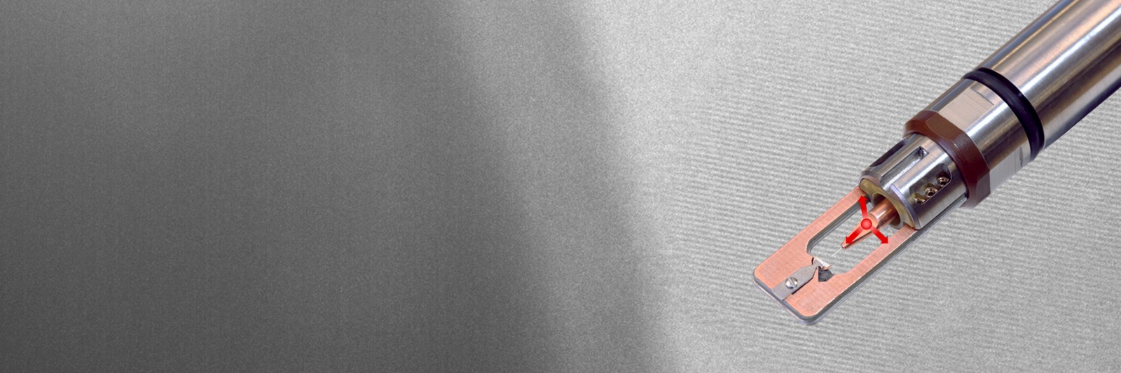
Create site-specific electrical contacts inside the TEM to study nanoscale devices, battery materials, nanowires, and 2D materials while correlating electrical measurements with real-time TEM/STEM characterization

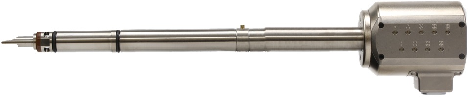
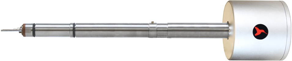
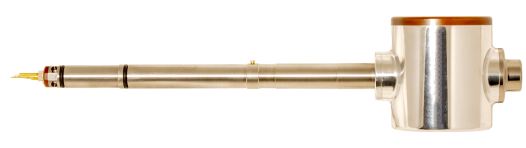
The Hummingbird Scientific TEM Biasing Nano-Manipulator Sample Holder enables site-specific nanomanipulation and electrical characterization during in-situ TEM and STEM experiments. Designed for researchers in semiconductor devices, nanotechnology, energy storage, materials science, electronics, and low-dimensional materials, it supports investigations of electrical transport, interface behavior, electrochemical reactions, device performance, nanowires, and 2D materials. By correlating localized electrical measurements with atomic-resolution imaging and analytical characterization, researchers can reveal the mechanisms governing electrical behavior, structural evolution, and device performance at the nanoscale.
Hummingbird Advantages:
- Precision movable probe for creating and repositioning site-specific electrical contacts with nanometer-scale positioning.
- Independent X, Y, and Z probe motion for accurate, repeatable sample navigation.
- Compatible with standard 3 mm half grids, FIB lift-out grids, and custom sample geometries.
- Easily replace standard commercially available STM probes to support diverse experimental requirements.
- Removable sample cartridge and dedicated setup block for simplified sample preparation and faster experiment setup.
- Full compatibility with TEM, STEM, SAED, EDS, and EELS during electrical characterization experiments.
Available For:

.jpg)

How it Works
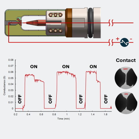
The TEM Biasing Nano-Manipulator Sample Holder combines a precision movable electrical probe, independent three-axis nanomanipulation, low-noise electrical connections, and an integrated source meter into a single platform for site-specific electrical characterization inside the TEM. Samples prepared on standard 3 mm half grids, FIB lift-out grids, or custom substrates are mounted in the removable sample cartridge using a dedicated setup block for accurate, repeatable assembly. The cartridge is then installed in the holder, automatically establishing electrical connections while leaving the measurement circuit open.
During the experiment, the movable probe is positioned using uncoupled piezo-driven coarse and fine motion along the X, Y, and Z axes until it contacts the specimen, completing the electrical circuit under direct TEM observation. Hummingbird Control™ Software provides an intuitive graphical user interface for precise probe control with configurable step sizes and integrated motion compensation to simplify contact formation and optimize probe positioning.
Once contact is established, researchers can apply electrical bias and acquire low-noise electrical measurements while simultaneously performing TEM/STEM imaging, electron diffraction, EDS, and EELS. The probe can be repositioned throughout the experiment to investigate multiple devices, interfaces, and regions within the same specimen, enabling flexible, site-specific electrical characterization in a single TEM session.
Key Features and Capabilities
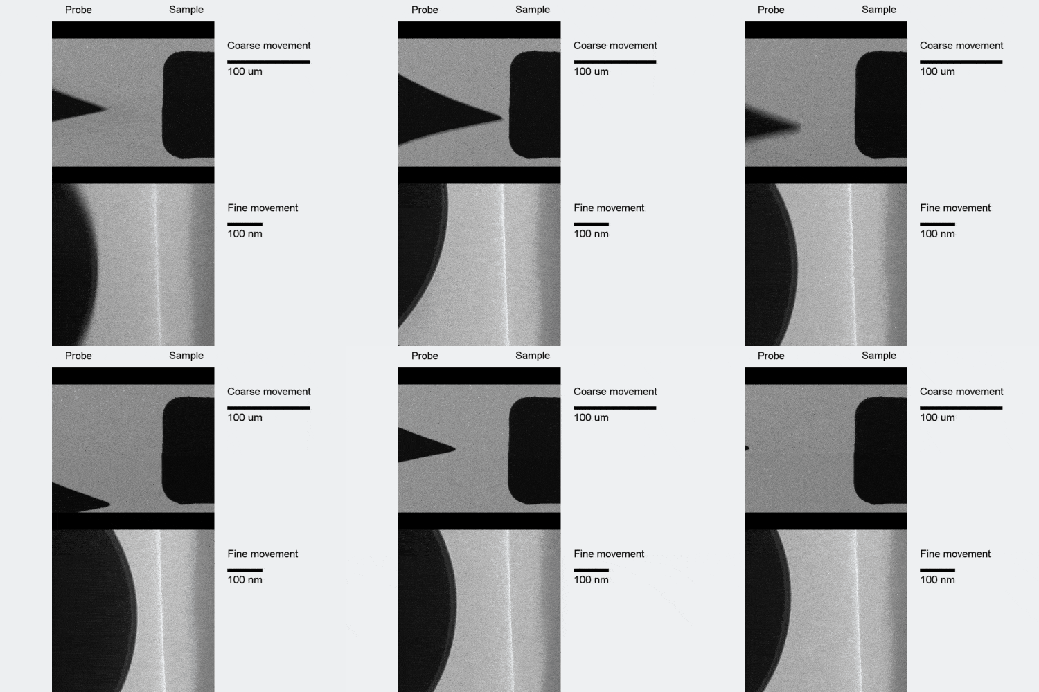
Position a movable electrical probe using precise uncoupled X, Y, and Z motion for site-specific electrical characterization
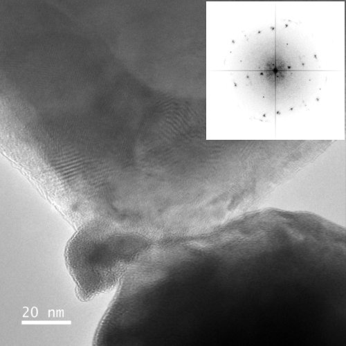
Preserve imaging stability while performing localized electrical measurements and analytical TEM characterization
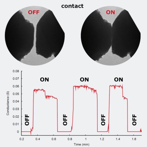
Acquire repeatable low-noise electrical measurements for accurate characterization of nanoscale materials and devices
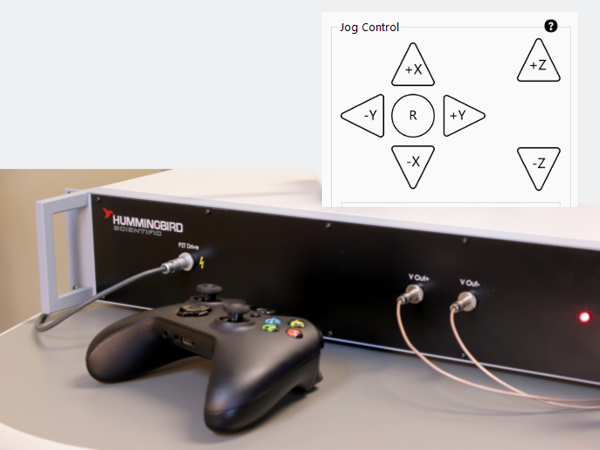
Control probe positioning and electrical measurements through integrated hardware and intuitive software
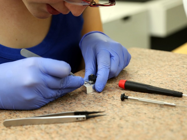
Simplify mounting of 3 mm half grids, FIB lift-out grids, and custom substrates with a dedicated sample loading fixture
Built for Diverse Research Applications

Featured Research

a) Charge/discharge profiles for interlayer cells. b) In-situ BF-TEM image of the Nanomanipulator probe prior to lithiation. c) Schematics of the cross-sectional morphologies that formed for Cu, Au, Ag, and Zn interlayers.
Operando TEM visualization of lithium plating and stripping in anode-less solid-state batteries
The Hummingbird Scientific TEM Biasing Nano-manipulator was used to directly observe lithium plating and stripping mechanisms in metal-interlayer-inserted anode-less solid-state lithium metal batteries based on Li6.5La3Zr1.5Ta0.5O12 solid electrolytes. The holder enabled operando electrical biasing and nanoscale imaging during electrochemical reactions, allowing researchers to correlate interfacial morphology changes with battery performance. By comparing Ag, Au, Cu, and Zn interlayers, the study revealed that Ag uniquely promoted stable lithium transport through a lithiated Ag interlayer, suppressing dendritic growth and maintaining interfacial contact during cycling. These operando observations provided direct insight into the influence of interlayer composition on plating behavior and interfacial stability in next-generation solid-state batteries.
Reference: Dong-Su Ko, et al. Nature Communications (2025). DOI:10.1038/s41467-025-55821-1
Copyright © 2025 The Author(s). Nature Communications published by Springer Nature. Open Access.
Video Spotlight
Video showing in-situ contact biasing of a nanobattery cell. Lithiation is observed directly upon contact while the novel composite electrode exhibited extroadniary stability during electrical cycling.
In-situ TEM of microstructural evolution in composite solid-state Li-ion batteries during charge/discharge cycles
Researchers at the University of Central Florida (UCF) have studied the structural integrity of a novel composite electrode composed of a polymer-derived ceramic nanoparticle and edge-functionalized graphene oxide during electrochemical lithiation and delithiation cycles.
They assembled a prototype nanobattery cell with a lithium metal and a SiCNO composite electrode and performed in-situ TEM lithation and delithation for at least two cycles using Hummingbird Scientific’s Biasing Manipulator TEM holder. The observed results demonstrated extraordinary structural stability of the SiCNO nanoparticles with only a 9.36% linear expansion during the lithiation (See Movie on the Left).
Hummngbird Advantages
- Movable probe allows site-specific biasing to observe localized electrochemical transformation
- Removable sample carrier with loading block for simplified sample preparation and mounting
- Easy exchange of widely-available commercial STM probes
- Control software with intuitie graphical user interface
Reference: Zhang et al. ACS Appl. Mater. Interfaces (2021) DOI: 10.1021/acsami.0c19681
Video Copyright © 2021 American Chemical Society
Software
Spend less time managing equipment and more time generating results. Hummingbird Control™ Software provides intuitive control of probe positioning and electrical measurements, including multi-axis motion, contact establishment, I–V characterization, voltage sweeps, live current and voltage plotting, and data export.
Hummingbird Connect™ can support the broader software strategy by connecting holder operation, nanomanipulation workflows, electrical characterization, TEM/STEM imaging, and experiment metadata. Together, these software tools help improve reproducibility, experiment setup, data organization, and long-term usability for probe-based in-situ TEM electrical characterization.
Built on Engineering Excellence
Hummingbird Scientific designs, machines, assembles, tests, and services its products in-house. Our integrated in-house engineering, precision manufacturing, microfabrication, software development, applications, and service teams enable rapid prototyping and iteration, custom modifications, and direct technical support throughout the life of the instrument.
The TEM Biasing Nano-Manipulator Sample Holder reflects this engineering approach by combining precision nanomanipulation, electrical biasing, and controller software and hardware technologies into a unified platform for reproducible in-situ TEM electrical characterization.
Need something unique? Our engineers can customize existing products or develop new solutions to support specialized probe designs, electrical configurations, sample geometries, and emerging research challenges.
Frequently Asked Questions
Related Products

Customization and Service